
Black box logic verification method for physical chip layout

A logic verification, chip technology, applied in electrical digital data processing, special data processing applications, instruments, etc., can solve problems such as power supply and ground short circuit

Active Publication Date: 2013-03-06
SHANGHAI HUAHONG GRACE SEMICON MFG CORP
View PDF7 Cites 5 Cited by
  • Summary
  • Abstract
  • Description
  • Claims
  • Application Information

AI Technical Summary

Problems solved by technology

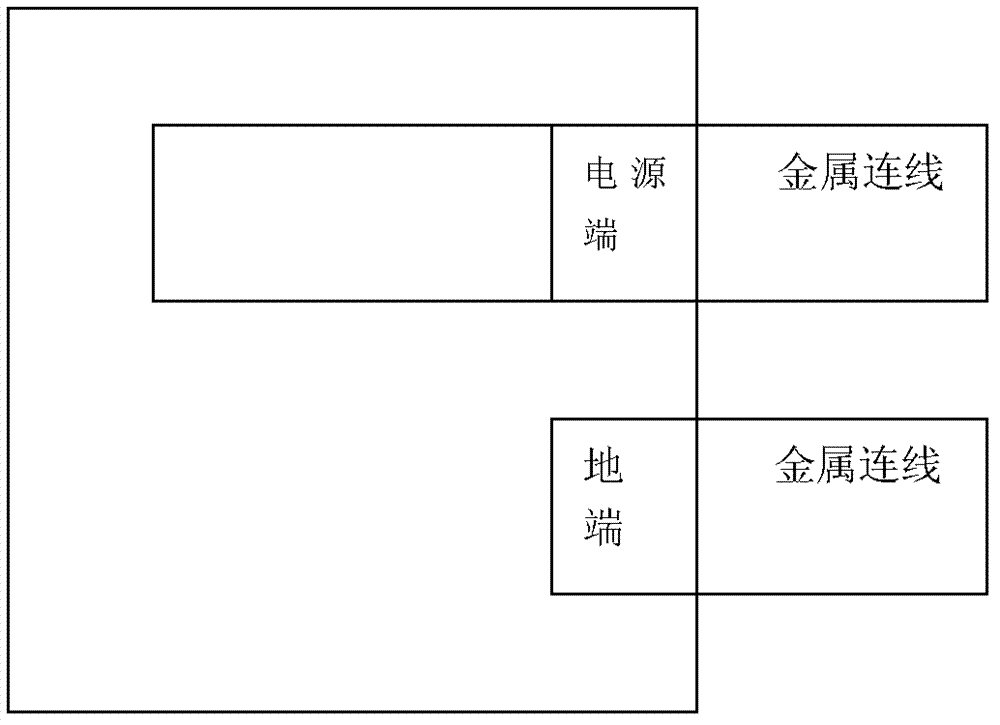
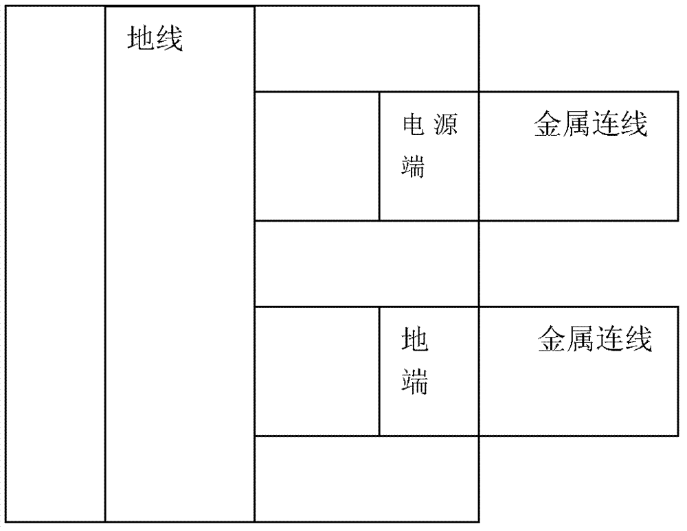
However, after the actual IP core is synthesized, it will be found that the power supply and the ground have been short-circuited, such as image 3 As shown, and the DRC metal level check will not report an error

Method used


Image

  • Black box logic verification method for physical chip layout
  • Black box logic verification method for physical chip layout
  • Black box logic verification method for physical chip layout

Examples


Embodiment Construction

[0023] Such as Figure 4 As shown, the black box logic verification method of the chip physical layout of the present invention is an improvement to the prior art BLACK BOX LVS (black box layout logic comparison) method, comprising the following steps:

[0024] The first step is to use the existing technology to conduct BLACK BOX LVS inspection on the chip;

[0025] The second step is to establish each process level library; through the established process level library, find out the information of the metal layer of the process and the information of the forbidden wiring layer, and store the information of each process metal layer and the information of the forbidden wiring layer, so that the program can use proceed to the next steps;

[0026] The third step is to read the GDSII data of the chip, and use the prohibited wiring layer as the identification feature to identify the position and name of each other party's IP in the chip;

[0027] The IP of the other party can be ...


PUM


Abstract

The invention discloses a black box logic verification method for physical chip layout. The method includes the steps: firstly, performing BLACK BOX LVS (layout versus schematic) checking for a chip; secondly, finding process metal layer information and keep-out layer information; thirdly, identifying position and name of each IP (internet protocol) of the other side in the chip; fourthly, extracting a keep-out layer of each IP of the other side to obtain a first data set; fifthly, extracting metal layer information in the chip, and rejecting the internal metal layer information of each IP of the other side in the chip by the aid of the name of each IP of the other side obtained in the third step so that a second data set is obtained; sixthly, subjecting the first data set and the second data set to 'logical conjunction'; and seventhly, comparing 'logical conjunction' results to find out short dots. The step of BLACK BOX upper metal connectivity verification checking is added after a user performs BLACK BOX LVS for the chip, and accordingly risk of short circuit of customer circuits and the IPs of the other side can be avoided.

Description

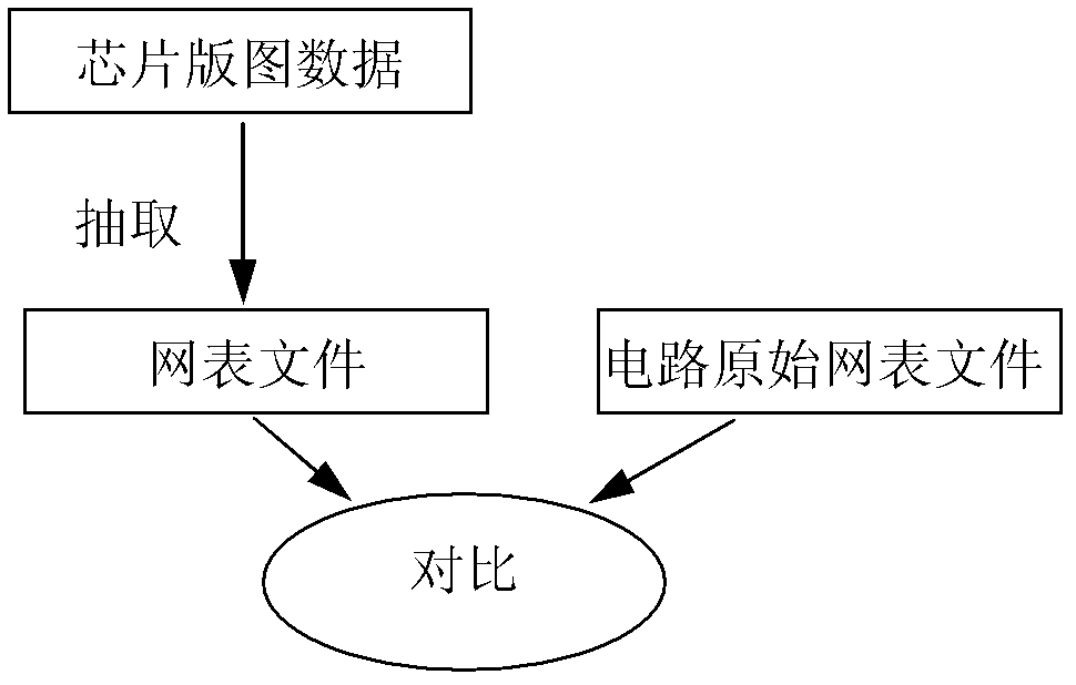
technical field [0001] The invention relates to a method for verifying the physical layout of a chip, in particular to a black-box logic verification method for the physical layout of the chip. Background technique [0002] After the chip layout design is completed, a logic comparison (LVS) between the circuit and the layout must be performed to ensure the consistency between the layout and the circuit. There are many EDA (Electronic Aided Design Software) manufacturers in the market that provide LVS tools. Such as figure 1 As shown, the basic idea of ​​LVS is to extract the physical layout, and compare the extracted circuit netlist with the designed circuit netlist. [0003] However, some chip units (such as IP) cannot do a complete LVS comparison. For example, when the IP is provided by another party, but the other party does not provide a complete physical layout of the IP core, only the PIN (input and output port) information of the IP is provided. At this time, the ...

Claims


Application Information

Patent Timeline
Patent Type & Authority Applications(China)
IPC IPC(8): G06F17/50
Inventor 潘炯倪凌云孙长江
Owner SHANGHAI HUAHONG GRACE SEMICON MFG CORP
Learn More