Novel flexible mechanical sensor and preparation method thereof
A sensor and flexible technology, applied in the field of new flexible mechanical sensors, can solve the problems of increased processes, poor film flexibility and air permeability, insufficient softness, etc., and achieves the effect of good piezoelectric performance, good air permeability, and reduced processes
- Summary
- Abstract
- Description
- Claims
- Application Information
AI Technical Summary
Problems solved by technology
Method used
Image

Examples
preparation example Construction
[0034] The method for preparing piezoelectric sensor of the present invention mainly comprises the following steps:
[0035] 1. Utilize organic solvent to prepare the solution to be spun of polyvinylidene fluoride or polyvinylidene fluoride-fluorinated olefin copolymer;
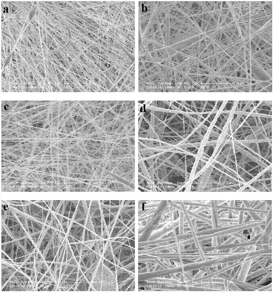
[0036] 2. Put the solution to be spun in an electrospinning device to stretch and polarize the solution to be spun to form a piezoelectric nanofiber film;
[0037] 3. Remove the remaining particles of the fiber film, and dry to remove the residual solvent;
[0038] 4. The processed fiber film and conductive film electrodes are assembled into a piezoelectric sensor device.
[0039] Electrospinning Technology
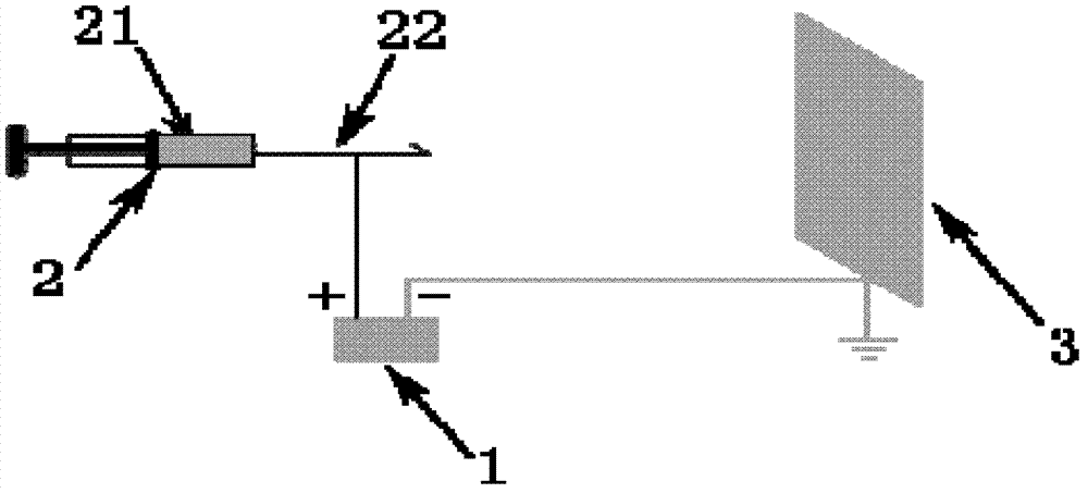
[0040] The method of the present invention is based on electrospinning technology, which is a novel technology for preparing nanofibers. figure 1 It is a schematic diagram of the structure of the electrospinning device, which includes:
[0041] High voltage power supply 1;
[0042] Injector 2 connec...
Embodiment approach
[0051]In the present invention, the conductive film electrode layer is preferably made of a conductive material with a flexible porous structure, which can be selected from traditional material electrodes prepared by etching techniques, including metal or metal oxide conductive films on flexible substrates, such as ITO-PET Film, etc.; carbon conductive film, including carbon conductive tape, graphene film, carbon nanotube film, etc.; conductive polymer film, including polypyrrole, polyacetylene, doped composite film, etc. According to the present invention, there is no limit to the selection of the material of the conductive film electrode layer, and those skilled in the art can select suitable materials according to specific applications, as long as it can be combined with the nanofiber film prepared by the present invention to form a piezoelectric sensor device, The thickness of the conductive film electrode layer matched with the fiber film is generally 100-1000nm.
[0052]...
Embodiment 1
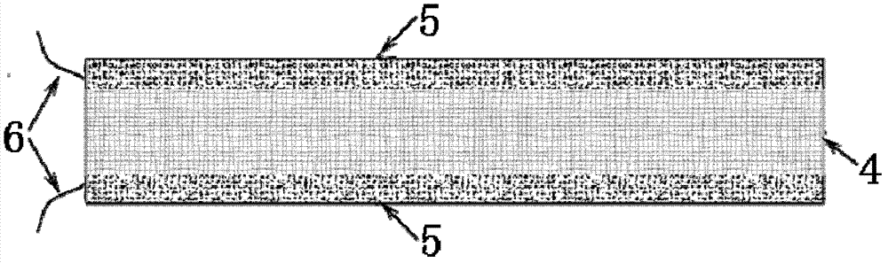
[0062] Using the mixture of dimethylformamide and acetone with a mass ratio of 4:6 as a solvent, a certain amount of PVDF powder was dissolved to prepare a solution to be spun with a concentration of 12% (w / v). Put the prepared solution in the liquid storage chamber of the injector, turn on the power supply of the spinning device, set the output voltage of the high-voltage power supply to 9kV, set the advancing speed of the injector solution to 1.2mL / h, and obtain the thickness on the receiving plate after 4 hours 30-40 micron fiber film. The fiber film obtained by spinning is dried for 6-8 hours, and combined with the upper and lower layers of ITO-PET film to obtain the following figure 2 The sensor device shown has a sensitivity of 30mV / N after a calibration test.
PUM
| Property | Measurement | Unit |
|---|---|---|
| Thickness | aaaaa | aaaaa |
| Thickness | aaaaa | aaaaa |
| Thickness | aaaaa | aaaaa |
Abstract
Description
Claims
Application Information
 - R&D
- Intellectual Property
- Life Sciences
- Materials
- Tech Scout
- Unparalleled Data Quality
- Higher Quality Content
- 60% Fewer Hallucinations
Browse by: Latest US Patents, China's latest patents, Technical Efficacy Thesaurus, Application Domain, Technology Topic, Popular Technical Reports.
© 2025 PatSnap. All rights reserved.Legal|Privacy policy|Modern Slavery Act Transparency Statement|Sitemap|About US| Contact US: help@patsnap.com