Copper electroplating composition and method of filling cavities in semiconductor substrates using same
A composition and semiconductor technology, applied in the direction of semiconductor devices, semiconductor/solid-state device manufacturing, circuits, etc.
- Summary
- Abstract
- Description
- Claims
- Application Information
AI Technical Summary
Problems solved by technology
Method used
Image

Examples
Embodiment 1
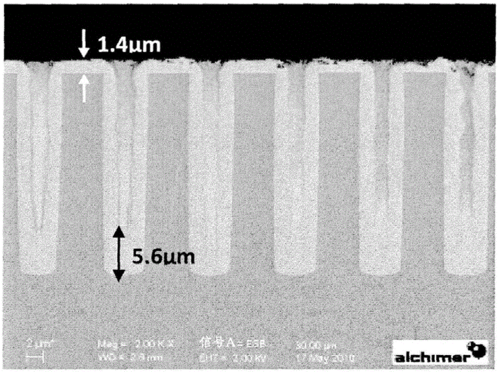
[0110] Example 1: Partial filling of holes with copper on a tantalum based barrier layer on which a copper seed layer has been deposited using an ethylenediamine-copper complex based composition according to the invention
[0111] A. Materials and equipment
[0112] Substrate:
[0113] The substrate used in this example was made of a 750 μm thick, 4 cm x 4 cm silicon wafer etched with a “through-hole” type cylindrical pattern with a depth of 25 μm and a diameter of 5 μm.
[0114] These patterns are covered with a 400nm thick layer of silicon dioxide, itself coated with a tantalum-based layer deposited by sputtering PVD (Physical Vapor Deposition), which is divided into two sublayers: the tantalum nitride sublayer layer (15nm) and tantalum sublayer (10nm).
[0115] This TaN / Ta "double layer" forms a copper diffusion barrier, such as is used in so-called "via" structures in integrated circuit fabrication.
[0116] A conformal copper seed layer with a thickness of about 200 nm...
Embodiment 2
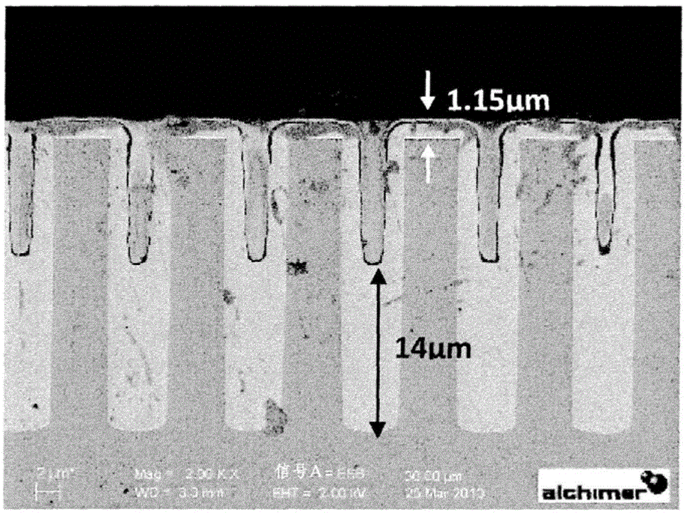
[0149] Example 2: Partial filling of holes with copper on a tantalum based barrier layer on which a copper seed layer has been deposited using an ethylenediamine-copper complex based composition according to the invention
[0150] A. Materials and equipment
[0151] Substrate:
[0152] The substrate used in this example is the same as that in Example 1.
[0153] Fill solution:
[0154] The solution used in this example is the same as that in Example 1.
[0155] equipment:
[0156] An electrowinning apparatus similar to fountain cells used in the microelectronics industry was used in this example.
[0157] An electrowinning cell contains an anode, which can be made of an inert metal such as platinum-coated titanium, or the same metal as the metal being deposited (copper in this case). A silicon wafer coated with a TaN / Ta barrier layer, itself coated with a copper seed layer, formed the cathode of the deposition cell.
Embodiment 4
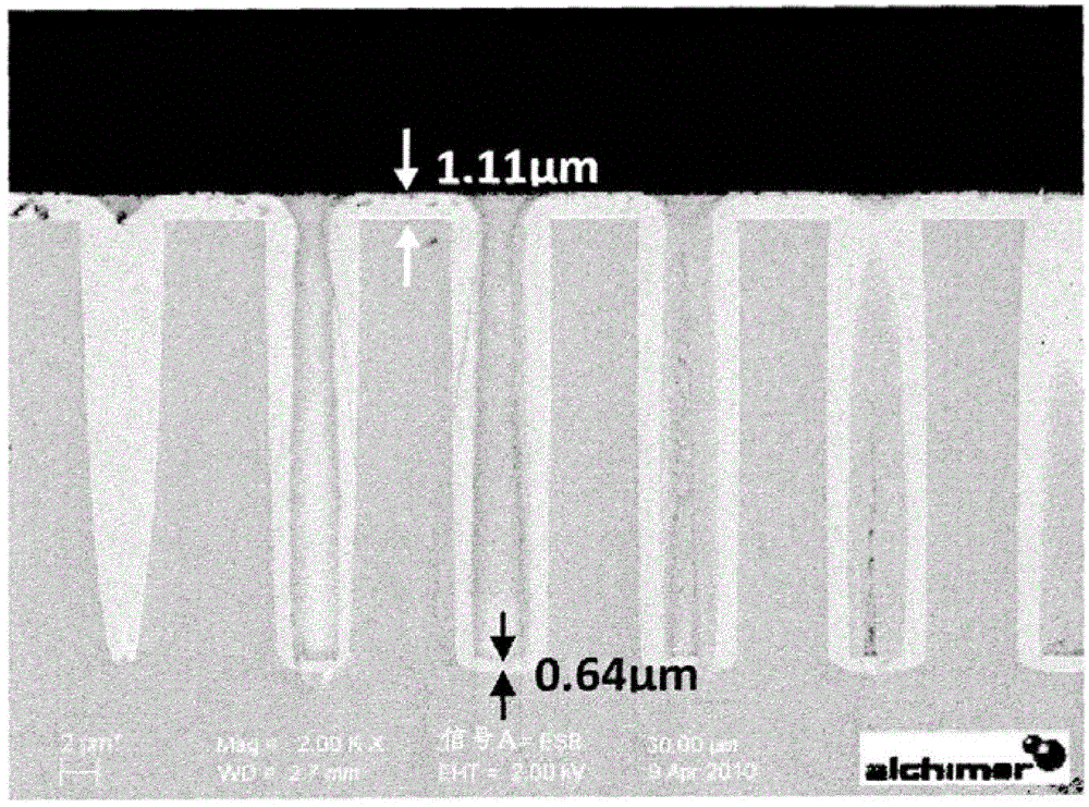
[0189] Example 4: Pore filling with copper on a nickel-based (NiB) barrier layer using an ethylenediamine-copper complex based composition according to the invention
[0190] A. Materials and equipment
[0191] Substrate:
[0192] The substrate used in this example consisted of a 750 μm thick, 4 cm x 4 cm doped (p-type) silicon wafer etched with “through hole” type cylindrical patterns of three different sizes:
[0193] - 25 μm in depth and 7 μm in diameter;
[0194] - 27 μm in depth and 9 μm in diameter; and
[0195] - 28 μm in depth and 11 μm in diameter.
[0196] Using the method described in document WO2010 / 001054, a 50 nm thick conformal NiB layer was deposited on the substrate surface, which layer formed a barrier to copper diffusion.
[0197] Fill solution:
[0198] The solution used in this example is the same as that in Example 1.
[0199] equipment:
[0200] The equipment used in this example is the same as that in Example 2.
[0201] B. Experimental method ...
PUM
| Property | Measurement | Unit |
|---|---|---|
| diameter | aaaaa | aaaaa |
| diameter | aaaaa | aaaaa |
| depth | aaaaa | aaaaa |
Abstract
Description
Claims
Application Information
 - R&D
- Intellectual Property
- Life Sciences
- Materials
- Tech Scout
- Unparalleled Data Quality
- Higher Quality Content
- 60% Fewer Hallucinations
Browse by: Latest US Patents, China's latest patents, Technical Efficacy Thesaurus, Application Domain, Technology Topic, Popular Technical Reports.
© 2025 PatSnap. All rights reserved.Legal|Privacy policy|Modern Slavery Act Transparency Statement|Sitemap|About US| Contact US: help@patsnap.com