Static random memory unit
A static random access memory and inverter technology, applied in the semiconductor field, can solve the problems of reducing the read and write speed of SRAM cells and difficult to guarantee the stability of SRAM read and write, so as to improve the read and write stability, suppress the single-event flip, and prolong the delay. effect of time
- Summary
- Abstract
- Description
- Claims
- Application Information
AI Technical Summary
Problems solved by technology
Method used
Image
Examples
Embodiment Construction
[0020] In order to better understand the technical content of the present invention, the preferred specific embodiments are illustrated as follows.
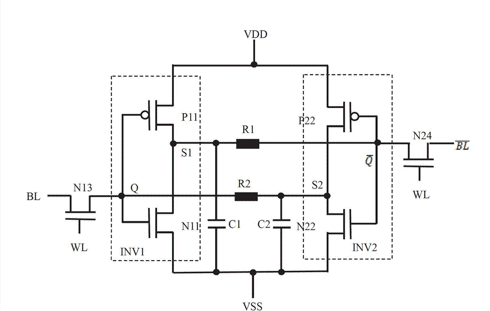
[0021] Please refer to Figure 4 , which shows a schematic structural diagram of the SRAM unit according to an embodiment of the present invention.
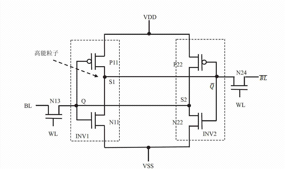
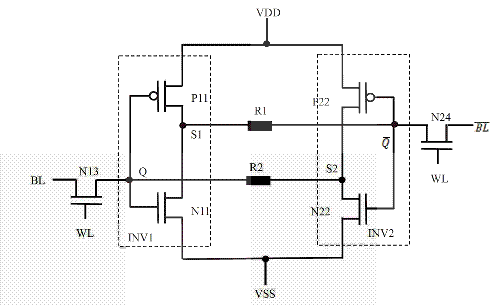
[0022] The SRAM unit of the present invention includes a first inverter INV1, a second inverter INV2, NMOS transmission gate transistors N13, N24, feedback resistors R1, R2 and feedback transistors T1, T2. The first inverter includes an NMOS transistor N11 and a PMOS transistor P11, and the second inverter INV2 includes an NMOS transistor N22 and a PMOS transistor P22. The drains of the NMOS transistor N11 and the PMOS transistor P11 are connected together as the output terminal S1 of the first inverter INV1 . The feedback resistor R1 and the feedback transistor T1 are coupled in parallel to the output terminal S1 of the first inverter INV1 and the input terminal of the second inv...
PUM
 Abstract
Description
Claims
Application Information
 - R&D
- Intellectual Property
- Life Sciences
- Materials
- Tech Scout
- Unparalleled Data Quality
- Higher Quality Content
- 60% Fewer Hallucinations
Browse by: Latest US Patents, China's latest patents, Technical Efficacy Thesaurus, Application Domain, Technology Topic, Popular Technical Reports.
© 2025 PatSnap. All rights reserved.Legal|Privacy policy|Modern Slavery Act Transparency Statement|Sitemap|About US| Contact US: help@patsnap.com


