Display device having plasmonic color filters and photovoltaic capabilities
A technology for plasma and display equipment, applied in the fields of filters, instruments, optics, etc., can solve problems such as light waste
- Summary
- Abstract
- Description
- Claims
- Application Information
AI Technical Summary
Problems solved by technology
Method used
Image
Examples
example 1
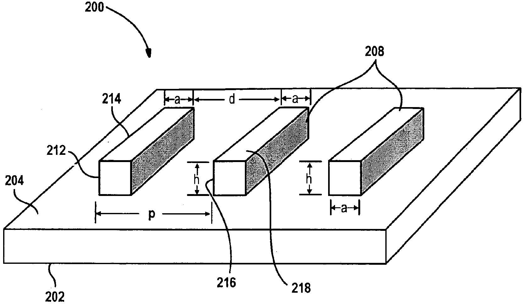
[0110] Gold nanogratings were fabricated as follows: Three types of large-area Au nanogratings with different periods (420 nm, 280 nm, and 220 nm) were fabricated by nanoimprint lithography (NIL-based) process. On a spin-cast MRI-8030 photoresist (Microresist Technology GmbH) on a glass substrate, at a pressure of 600 psi and a temperature of 180 °C for 5 min, SiO with a duty cycle of 0.7 2 Dies were NIL performed in a Nanonex NX 2000 nanoimprinter (Princeton, NJ). After cooling, the mold was demolded, and Ti was selectively deposited on each sidewall of the embossed grating structure by angled deposition. Ti deposited onto the photoresist pattern, in O 2 The barb structure is induced during reactive ion etching (RIE), which facilitates the lift-off process. o 2 RIE (20 sccm O 2 , 12mTorr chamber pressure and 30W bias power), deposit 40nm Au and 1nm Ti, use electron beam evaporator and lift-off process to complete the fabrication of Au nano-grating structure on the substra...
example 2
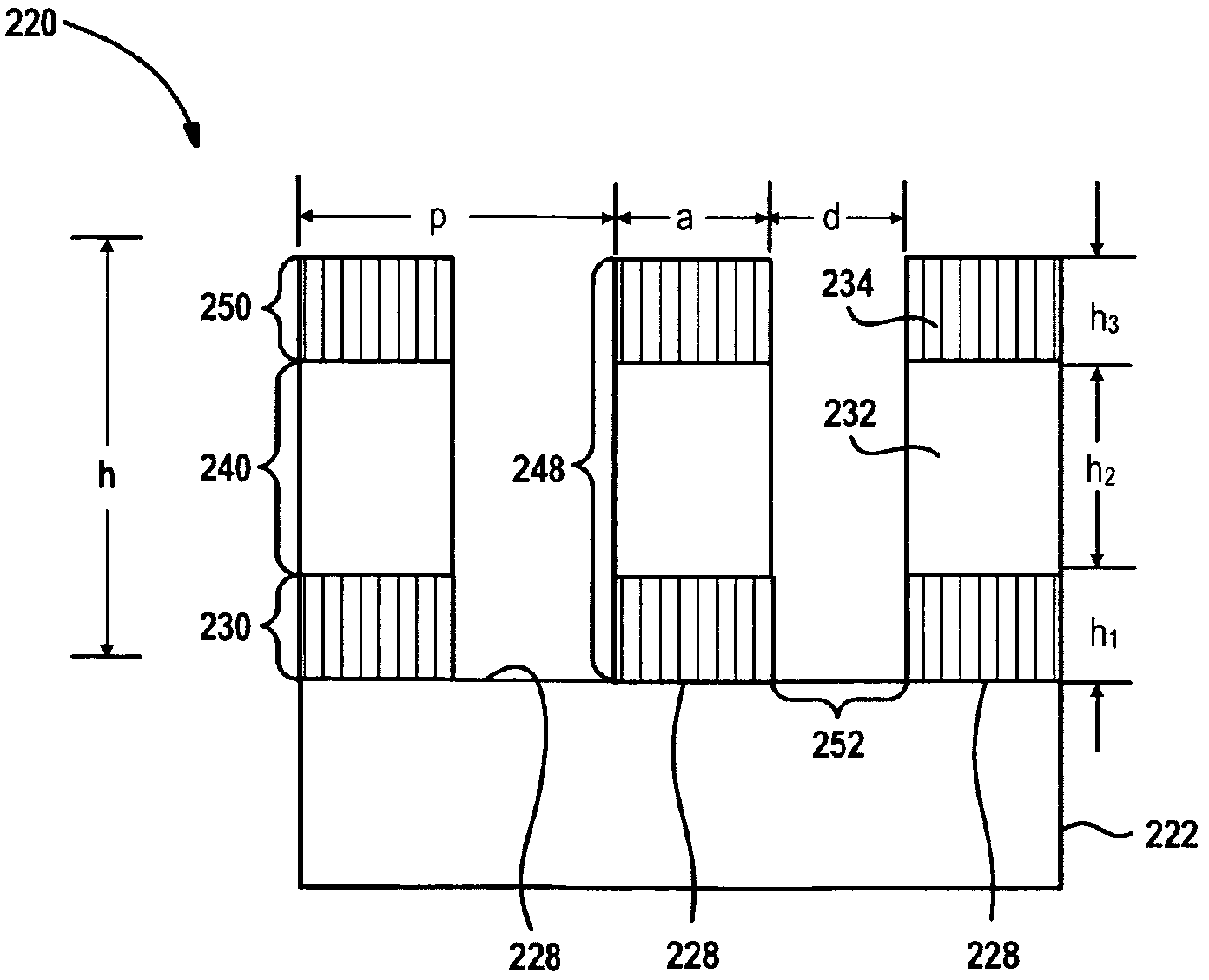
[0114] Plasmonic nanoresonator devices for color filtering, as above Figure 10A As discussed in , is formed as follows. For ease of manufacture, the device is designed to operate on magnesium fluoride (MgF 2 ) Subwavelength periodic MIM stack arrays on transparent films. Glass substrates are prepared using a clean process. Using an electron beam evaporator, at 0.5nms -1 At a deposition rate of 220nm magnesium fluoride layer (MgF 2 ), 40nm of Al, 100nm of zinc selenide (ZnSe) and another 40nm of Al. To prevent the oxidation of Al, the samples were stored in an oxygen-free glove box before measurement. For each stack, a 100nm thick zinc selenide (ZnSe) dielectric layer is sandwiched between two 40nm thick aluminum (Al) grating layers. The duty cycle of the stacked array is about 0.7.
[0115] Patterned and milled using a focused ion beam in a Nova NanoLab DuaLbeam workstation (FEI). Milling is controlled using an automated FIB program provided by FEI that controls all r...
example 3
PUM
 Abstract
Description
Claims
Application Information
 - R&D
- Intellectual Property
- Life Sciences
- Materials
- Tech Scout
- Unparalleled Data Quality
- Higher Quality Content
- 60% Fewer Hallucinations
Browse by: Latest US Patents, China's latest patents, Technical Efficacy Thesaurus, Application Domain, Technology Topic, Popular Technical Reports.
© 2025 PatSnap. All rights reserved.Legal|Privacy policy|Modern Slavery Act Transparency Statement|Sitemap|About US| Contact US: help@patsnap.com


