Method for preparing micro-nano structure on material surface based on laser interference photolithography

A technology of laser interference lithography and micro-nano structure, which is applied in the field of electronics, can solve the problems of inability to mass-produce large-area micro-nano patterns with flexible cycle scales, and high cost due to size limitations of photolithography methods, achieving wide application and low cost. cheap effect

Inactive Publication Date: 2012-12-26
FUDAN UNIV
View PDF5 Cites 12 Cited by
  • Summary
  • Abstract
  • Description
  • Claims
  • Application Information

AI Technical Summary

Problems solved by technology

[0002] Fabricating micro-nano structures with specific structures on the surface of materials has always been the focus of research in the field of microelectronics and nanoscience. However, due to the size limitation and high cost of traditional photolithography methods, it is impossible to mass-produce micro-nano patterns with large areas and flexible periodic scales. , and the fabrication of these specific periodic structures is a core technology in the fields of microelectronic device fabrication, biomedicine, and electronic detection, so low-cost mass production of large-area micro-nano structures has extremely high market value

Method used


Image

  • Method for preparing micro-nano structure on material surface based on laser interference photolithography
  • Method for preparing micro-nano structure on material surface based on laser interference photolithography
  • Method for preparing micro-nano structure on material surface based on laser interference photolithography

Examples


Embodiment Construction

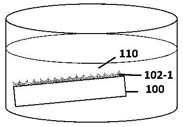
[0021] Hereinafter, the present invention is described more specifically in reference examples with reference to the drawings, and the present invention provides preferred embodiments, but should not be construed as being limited to the embodiments set forth herein. In the drawings, the thicknesses of layers and regions are exaggerated for convenience of illustration, and the shown sizes do not represent actual sizes.

[0022] The reference figure is a schematic diagram of an idealized embodiment of the present invention, and the embodiment shown in the present invention should not be considered limited to the specific shape of the region shown in the figure. In the embodiment of the present invention, a more complex array of nano needle points Structural representation, other simple structures, such as gratings, lattices, etc., are included in the present invention, and the representation in the figure is schematic, but this should not be considered as limiting the scope of th...


PUM


Abstract

The invention belongs to the technical field of electronics, and particularly relates to a method for preparing a micro-nano structure on a material surface based on laser interference photolithography. The micro-nano structure is formed on photoresist by generation of laser interference, so as to transfer the micro-nano structure on the photoresist to the material surface of a substrate with an etching method, and form the structures such as micro-nano-scale gratings, dot matrixes and linear arrays. By adoption of the method disclosed by the invention, high-quality nano structures can be produced in a large area on various material surfaces. The method disclosed by the invention is simple and convenient, is low in cost and has a great application value.

Description

technical field [0001] The invention belongs to the field of electronic technology, and in particular relates to a method for fabricating a micro-nano structure on a material surface by using laser interference lithography. Background technique [0002] Fabricating micro-nano structures with specific structures on the surface of materials has always been the focus of research in the field of microelectronics and nanoscience. However, due to the size limitation and high cost of traditional photolithography methods, it is impossible to mass-produce micro-nano patterns with large areas and flexible periodic scales. , and the fabrication of these specific periodic structures is a core technology in the fields of microelectronic device fabrication, biomedicine, and electronic detection. Therefore, low-cost mass production of large-area micro-nano structures has extremely high market value. [0003] The method of laser interference lithography has incomparable advantages in the ma...

Claims


Application Information

Patent Timeline
Patent Type & Authority Applications(China)
IPC IPC(8): B81C1/00G03F7/20
Inventor 于航陆冰睿刘冉
Owner FUDAN UNIV
Why Eureka
Try Eureka