
Printed circuit board laminating structure and laminating method

A technology for printed circuit boards and circuit boards, applied in the directions of printed circuits, printed circuits, printed circuit manufacturing, etc., can solve the problems of difficult structural design and lack of competitive advantages, so as to reduce the difficulty of structural design, suitable for popularization and application, Simple preparation method

Inactive Publication Date: 2012-12-12
GUANGDONG OPPO MOBILE TELECOMM CORP LTD
View PDF3 Cites 7 Cited by
  • Summary
  • Abstract
  • Description
  • Claims
  • Application Information

AI Technical Summary

Problems solved by technology

[0003] And cost is often the primary problem that must be faced in the design of communication digital products. Without cost advantage, there may be no competitive advantage
At the same time, with the thinning and thinning of communication digital products, the structural design is becoming more and more difficult. If the use of connectors is increased, the product thickness, strength and difficulty will inevitably be sacrificed.

Method used


Image

  • Printed circuit board laminating structure and laminating method
  • Printed circuit board laminating structure and laminating method
  • Printed circuit board laminating structure and laminating method

Examples


Embodiment 1

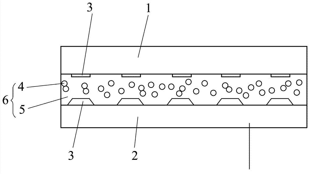
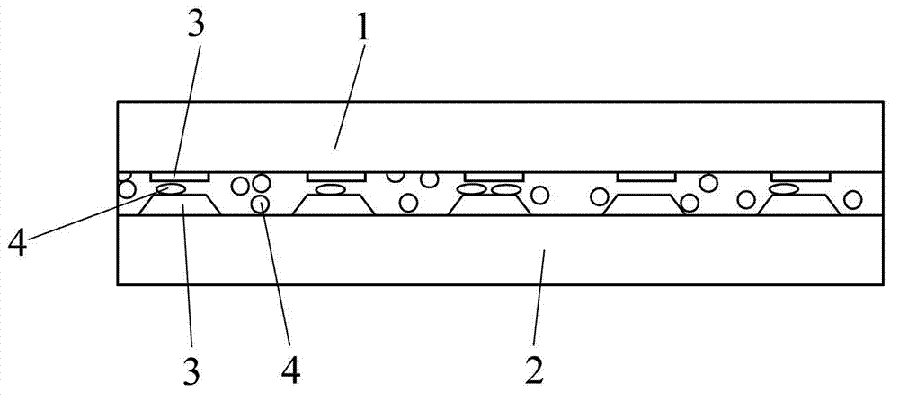
[0020] refer to figure 1 and figure 2 , a printed circuit board pressing structure, including two circuit boards 1 and 2, the two circuit boards are discontinuously provided with opposite golden fingers 3, conductive particles 4 and resin adhesive are distributed between the two circuit boards The conductive adhesive 6 composed of 5, by pressurizing and heating the circuit boards, the conductive particles 4 are broken at the opposite positions of the gold fingers 3 on the two circuit boards, and squeezed together to form conduction without the position of the gold fingers The conductive particles 4 are not broken and conduction is not formed.

[0021] The conductive adhesive is anisotropic conductive adhesive, referred to as ACF adhesive, and its full name is Anisotropic Conductive Film. It is a translucent polymer continuous material with three characteristics of adhesion, conductivity, and insulation. It conducts electricity in the Z direction, and X, Y directions Non-con...

Embodiment 2

[0028] refer to figure 1 and figure 2 , a printed circuit board pressing structure, including two circuit boards 1 and 2, the two circuit boards are discontinuously provided with opposite golden fingers 3, conductive particles 4 and resin adhesive are distributed between the two circuit boards The conductive adhesive 6 composed of 5, by pressurizing and heating the circuit boards, the conductive particles 4 are broken at the opposite positions of the gold fingers 3 on the two circuit boards, and squeezed together to form conduction without the position of the gold fingers The conductive particles 4 are not broken and conduction is not formed.

[0029] The conductive adhesive is anisotropic conductive adhesive, referred to as ACF adhesive, and its full name is Anisotropic Conductive Film. It is a translucent polymer continuous material with three characteristics of adhesion, conductivity, and insulation. It conducts electricity in the Z direction, and X, Y directions Non-con...


PUM


Abstract

The invention provides a printed circuit board laminating structure, comprising two circuit boards, wherein bonding fingers on the circuit boards are connected in a laminating manner; conducting adhesive composed of conducting particles and a resin bonding agent is distributed between the bonding fingers; through pressurizing and heating the conducting adhesive, the conducting particles are broken at positions where the bonding fingers are connected, and extruded together to form a break-over, however the conducting particles at the positions without the bonding fingers are not broken to form the break-over. By the printed circuit board laminating structure, costs which are increased by a reason of adding a connector are reduced, and the structure design difficulty and the costs which are increased by a rigid-flexible board are reduced.

Description

technical field [0001] The present invention relates to the technical field of printed circuit boards, in particular to a printed circuit board lamination structure and lamination method. Background technique [0002] In some communication digital products today, in the connection of printed circuit boards, connectors are often used, or interconnection is achieved by making soft and hard boards. However, the use of connectors increases the difficulty of structural design and the cost of connectors. Although the technology of rigid-flex boards is more mature and reliable, the cost of rigid-flex boards is lower than that of pure hard boards or soft boards due to the limitation of the manufacturing process. Boards are about 50% more expensive. [0003] And cost is often the primary problem that must be faced in the design of communication digital products. Without cost advantage, there may be no competitive advantage. At the same time, with the thinning and thinning of commun...

Claims


Application Information

Patent Timeline
Patent Type & Authority Applications(China)
IPC IPC(8): H05K1/11H05K3/40
CPCH05K2201/0221H05K3/36H05K3/323
Inventor 傅雪峰
Owner GUANGDONG OPPO MOBILE TELECOMM CORP LTD
Learn More