
A fully-mode double-ridge substrate integrated waveguide with balanced microstrip line transition

A technology of balanced microstrip lines and integrated waveguides, applied in waveguides, waveguide-type devices, circuits, etc., can solve problems such as narrow single-mode operating bandwidth, achieve low equivalent impedance, reduced frequency range, and high multi-mode propagation coefficients Effect

Active Publication Date: 2014-10-01
HARBIN INST OF TECH
View PDF8 Cites 0 Cited by
  • Summary
  • Abstract
  • Description
  • Claims
  • Application Information

AI Technical Summary

Problems solved by technology

[0003] In order to solve the problem of narrow single-mode working bandwidth of the existing dielectric integrated waveguide, the present invention further proposes a full-mode double-ridge substrate integrated waveguide with balanced microstrip line transition

Method used


Image

  • A fully-mode double-ridge substrate integrated waveguide with balanced microstrip line transition
  • A fully-mode double-ridge substrate integrated waveguide with balanced microstrip line transition
  • A fully-mode double-ridge substrate integrated waveguide with balanced microstrip line transition

Examples


specific Embodiment approach 1

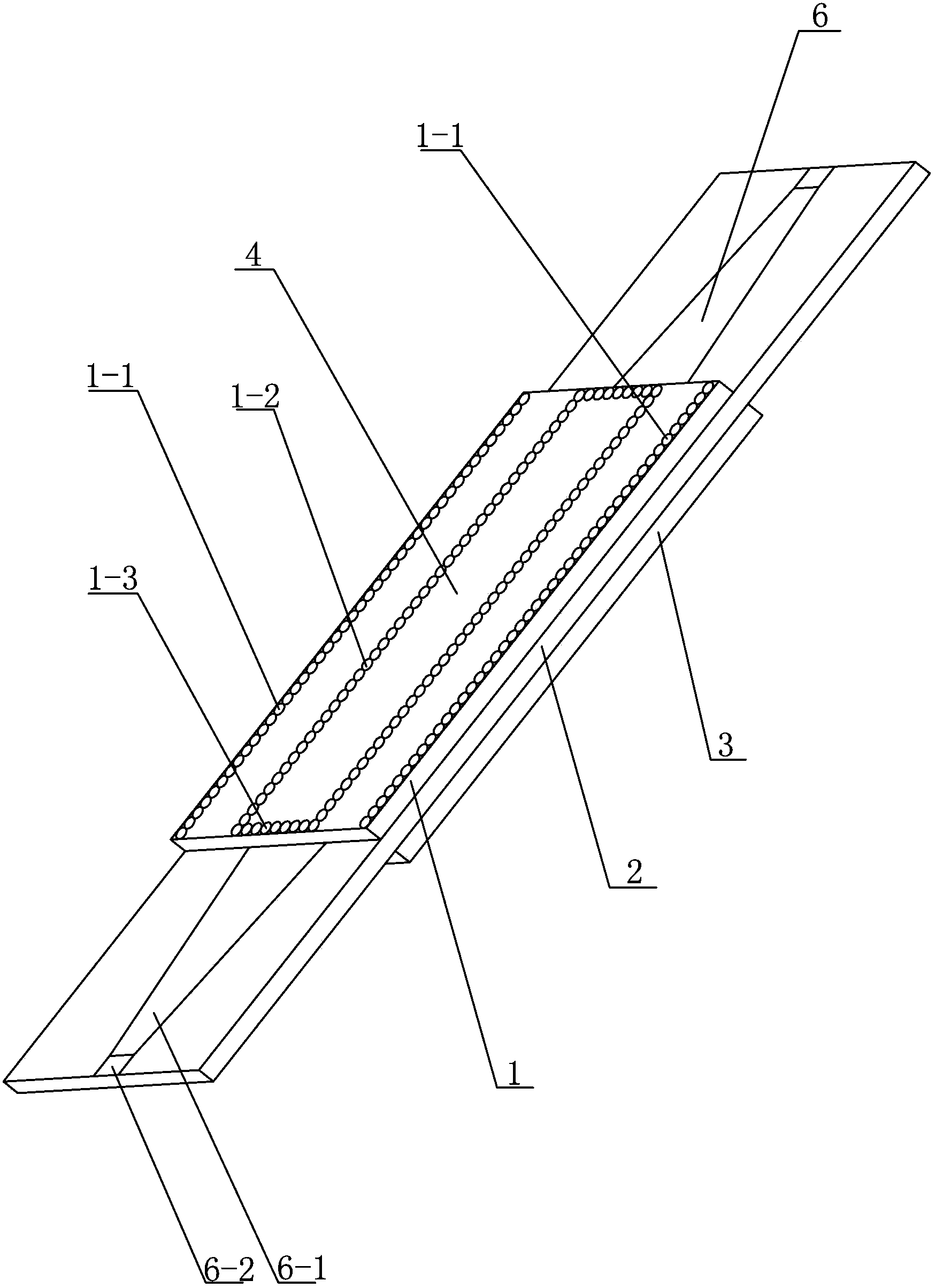
[0007] Specific implementation mode 1: Combination Figure 1 to Figure 4 To illustrate this embodiment, a full-mode dual-ridge substrate integrated waveguide with balanced microstrip line transition described in this embodiment includes an upper dielectric substrate 1, a middle dielectric substrate 2, a lower dielectric substrate 3, and an upper metal patch 4. , The lower metal patch 5 and four balanced microstrip lines 6, the upper surface and the lower surface of the middle dielectric substrate 2 are respectively pasted with a metal strip, the upper dielectric substrate 1, the middle dielectric substrate 2, the lower dielectric substrate The sheets 3 are stacked in sequence from top to bottom, and the two ends of the middle dielectric substrate 2 are exposed. The upper metal patch 4 is attached to the upper surface of the upper dielectric substrate 1, and the lower metal patch 5 is attached to the lower layer. On the lower surface of the dielectric substrate 3, a balanced micr...

specific Embodiment approach 2

[0008] Specific implementation manner two: combination Figure 1 to Figure 4 To illustrate this embodiment, each balanced microstrip line 6 of a full-mode dual-ridge substrate integrated waveguide with balanced microstrip line transition described in this embodiment is composed of an isosceles trapezoidal plate 6-1 and a rectangular plate 6-2. One side of the rectangular plate 6-2 is integrally connected with the short base of the isosceles trapezoidal plate 6-1, and the long base of the isosceles trapezoidal plate 6-1 is connected with a metal strip located on the same plane. The other components and connection relationships are the same as in the first embodiment.

specific Embodiment approach 3

[0009] Specific implementation mode three: combination Figure 2 to Figure 4 To illustrate this embodiment, the length W4 of the short base of the isosceles trapezoidal plate 6-1 of each balanced microstrip line 6 of the full-mode dual-ridge substrate integrated waveguide of the balanced microstrip line transition described in this embodiment is The length W5 of the long base of the isosceles trapezoidal plate 6-1 is 18 mm, and the height L4 of the isosceles trapezoidal plate 6-1 is 30 mm. Other components and connection relationships are the same as in the second embodiment.


PUM


Abstract

The invention relates to a full-mode double-ridge substrate integrated waveguide, in particular to a full-mode double-ridge substrate integrated waveguide in balanced microstrip line transition, aiming to solve the problem that the single-mode working bandwidth of the conventional medium integrated waveguide is relatively narrow. Metal strips are adhered to the upper surface and the lower surface of a middle medium substrate of the full-mode double-ridge substrate integrated waveguide in the balanced microstrip line transition respectively; an upper medium substrate, the middle medium substrate and a lower medium substrate are sequentially laminated from the top down; two end parts of the middle medium substrate are exposed; balanced microstrip lines are adhered to the upper surface and the lower surface of the two end parts of the middle medium substrate respectively; each second upper metallizing through hole and each third upper metallizing through hole are connected with an upper metal adhering sheet and the metal strip on the upper surface of the middle medium substrate respectively to form an upper ridge; and each second lower metallizing through hole and each third lower metallizing through hole are connected with a lower metal adhering sheet and the metal strip on the lower surface of the middle medium substrate respectively to form a lower ridge. The full-mode double-ridge substrate integrated waveguide in the balanced microstrip line transition is used in the field of radio technology.

Description

Technical field [0001] The invention relates to a full-mode dual-ridge substrate integrated waveguide, in particular to a full-mode dual-ridge substrate integrated waveguide with balanced microstrip line transition. Background technique [0002] The traditional metal rectangular waveguide has low loss and high power capacity and has been widely used in the microwave field, but it is a non-planar structure and has the disadvantages of being difficult to integrate with a planar printed circuit board. Printed circuit technology has received extensive attention due to its compact structure and easy integration with communication systems. The dielectric integrated waveguide structure integrates metal rectangular waveguide and planar printed circuit technology, and thus has been widely used in the communication field. The dielectric integrated waveguide structure has many advantages of traditional rectangular waveguides. It can be printed on a flat circuit board with low loss and struc...

Claims


Application Information

Patent Timeline
Patent Type & Authority Patents(China)
IPC IPC(8): H01P3/18
Inventor 林澍田雨陆加刘曦马欣茹赵志华王力卓王立娜
Owner HARBIN INST OF TECH
Learn More