Preparation method of graphene-carbon nano tube composite structure
A technology of carbon nanotube compounding and graphene compounding, which is applied in the direction of graphene, single-layer graphene, nano-carbon, etc., can solve the problem of poor conductivity, toughness and light transmittance, decreased conductivity of composite structures, and affecting the toughness of composite structures, etc. problems, to achieve the effect of low equipment requirements, excellent conductivity, and simple operation
- Summary
- Abstract
- Description
- Claims
- Application Information
AI Technical Summary
Problems solved by technology
Method used
Image
Examples
specific Embodiment 1
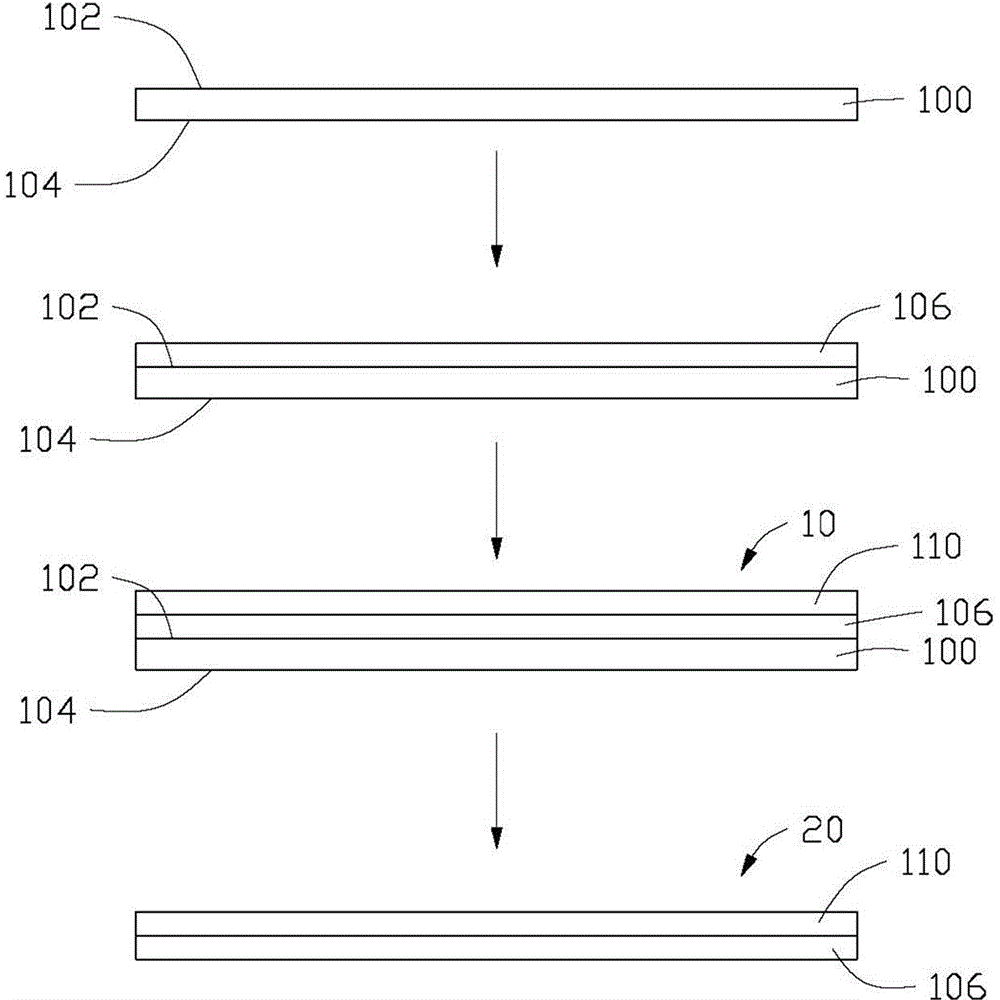
[0023] See figure 1 , the preparation method of the graphene-carbon nanotube composite structure 20 provided by the specific embodiment of the present invention comprises the following steps:
[0024] Step 1, providing a substrate 100 having a first surface 102 and a second surface 104 opposite to the first surface 102 .
[0025] The substrate 100 can be made of metal materials, such as copper, nickel, etc., or non-metallic materials, such as quartz plates, glass, plastics, tapes, etc. The first surface 102 of the substrate 100 may have an oxide layer. The length, width and thickness of the base body 100 are not limited and can be adjusted as required. The first surface 102 can be a plane or a curved surface. In this embodiment, the material of the substrate 100 is a silicon wafer. The silicon wafer is a cuboid structure with a thickness of 12.5 microns to 50 microns, preferably 25 microns, and a side length of 4 cm. The first surface 102 is a square plane with a side len...
specific Embodiment 2
[0073] See Figure 11 , the preparation method of the graphene-carbon nanotube composite structure 20 provided in the second embodiment of the present invention comprises the following steps:
[0074] Step 1, providing a substrate 100 having a first surface 102 and a second surface 104 opposite to the first surface 102 .
[0075] Step 2. At least one graphene film 106 is provided, and the graphene film 106 is formed or disposed on the first surface 102 of the substrate 100 .
[0076] Step 3, coating the protective layer 108 on the graphene film 106 on the first surface 102 of the substrate 100 .
[0077] Step 4, removing the matrix 100 to obtain a protective layer-graphene composite structure 40 .
[0078] Step 5, at least one carbon nanotube layer 110 is provided, the protective layer-graphene composite structure 40 is compounded with the carbon nanotube layer 110, and the graphene film 106 is in contact with the carbon nanotube layer 110 to obtain Protective layer-graphen...
PUM
| Property | Measurement | Unit |
|---|---|---|
| visible light transmittance | aaaaa | aaaaa |
| aperture size | aaaaa | aaaaa |
| diameter | aaaaa | aaaaa |
Abstract
Description
Claims
Application Information
 - R&D
- Intellectual Property
- Life Sciences
- Materials
- Tech Scout
- Unparalleled Data Quality
- Higher Quality Content
- 60% Fewer Hallucinations
Browse by: Latest US Patents, China's latest patents, Technical Efficacy Thesaurus, Application Domain, Technology Topic, Popular Technical Reports.
© 2025 PatSnap. All rights reserved.Legal|Privacy policy|Modern Slavery Act Transparency Statement|Sitemap|About US| Contact US: help@patsnap.com


