One-dimensional photonic crystal double-prism defect dispersion separator

A technology of one-dimensional photonic crystals and double prisms, which is applied in the directions of light guide, optics, instruments, etc., can solve the problems of difficult assembly and adjustment, poor stability, large size and weight of devices, and achieves good plasticity, high spatial resolution, and preparation technology. mature effect

Inactive Publication Date: 2012-11-21
JIANGSU UNIV
View PDF4 Cites 2 Cited by
  • Summary
  • Abstract
  • Description
  • Claims
  • Application Information

AI Technical Summary

Problems solved by technology

[0002] Due to the disadvantages of difficult assembly and adjustment, large device volume and weight, and poor stability, the traditional discrete optical device system can no longer meet the needs of the development of modern information optoelectronic technology. New principles, new concepts, and new structural designs of some devices have been proposed one after another. Such as photonic crystals, micro-resonators, micro-cavity lasers, nano-quantum wire light guides, plasmonic surface waves, etc.

Method used


Image

  • One-dimensional photonic crystal double-prism defect dispersion separator
  • One-dimensional photonic crystal double-prism defect dispersion separator
  • One-dimensional photonic crystal double-prism defect dispersion separator

Examples


Embodiment Construction

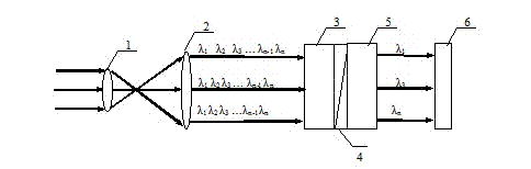
[0025] figure 1 It is a schematic diagram of a one-dimensional photonic crystal double prism defect dispersion separator system. After the multi-wavelength incident beam is focused by the focusing prism 1, it is expanded by the confocal beam expander prism 2 and projected on the surface of the one-dimensional photonic crystal, passing through the high and low refractive index periodic dielectric layers 3 and 5 with the double prism defect layer 4 to realize defect filtering , different positions only allow a certain wavelength to pass through, so that different wavelengths λ 1 lambda 2 lambda 3 ...λ n-1 lambda n The waves are separated in space and projected onto the detector 6 to form a fine spectral structure.

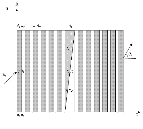
[0026] The one-dimensional photonic crystal is modeled, and the model parameters are set. The specific implementation is as follows: a double prism structure is set in a complete one-dimensional photonic crystal to form a one-dimensional photonic crystal...


PUM

PropertyMeasurementUnit
Thicknessaaaaaaaaaa
Thicknessaaaaaaaaaa
Refractive indexaaaaaaaaaa

Abstract

The invention discloses a multi-wavelength signal dispersion separation method by using defective one-dimensional photonic crystals and relates to the field of spectral measurement. Based on photonic band gap and defect filter characteristics of the one-dimensional photonic crystals, by introducing double-prism defect layers into perfect one-dimensional photonic crystals to enable the thickness of the double-prism defect layers to be varied continuously, different positions correspond to different defect structures, a one-to-one corresponding relationship is formed between the output spectral lines and input and output positions, a characteristic of frequency separating is realized on multi-wavelength electromagnetic waves and a superfine spectral structure is formed. The one-dimensional photonic crystal double-prism defect dispersion separator has very high spectral resolution and can be used on devices such as wave separators and spectrographs; and at the same time, by adopting a thin film preparation technology, the one-dimensional photonic crystal double-prism defect dispersion separator can be integrated with other devices and the preparation technique is mature.

Description

technical field [0001] The invention relates to a one-dimensional photonic crystal dispersion separator, which has frequency separation characteristics for multi-wavelength electromagnetic waves and forms ultra-fine spectral structures. Background technique [0002] Due to the disadvantages of difficult assembly and adjustment, large device volume and weight, and poor stability, the traditional discrete optical device system can no longer meet the needs of the development of modern information optoelectronic technology. New principles, new concepts, and new structural designs of some devices have been proposed one after another. Such as photonic crystals, micro-resonators, micro-cavity lasers, nano-quantum wire light guides, plasmonic surface waves, etc. In recent years, a large number of studies have shown that photonic crystals have broad application prospects, especially in the fields of optical communication and optical information processing. Photonic crystals can b...

Claims


Application Information

Patent Timeline
IPC IPC(8): G02B27/10G02B6/122
Inventor 高永锋任乃飞许孝芳周明王正岭刘红玉
Owner JIANGSU UNIV
Why Eureka
Try Eureka