Electrode structure with grid lines on front surface
An electrode structure, front grid line technology, applied in circuits, electrical components, semiconductor devices, etc., can solve the problem that the amount of paste used has not been reduced as expected, the battery efficiency has not been further improved, and the bus line is easy to print and offset. and other problems, to achieve the effect of improving the photoelectric conversion efficiency, reducing the paste and reducing the area.
- Summary
- Abstract
- Description
- Claims
- Application Information
AI Technical Summary
Problems solved by technology
Method used
Image
Examples
Embodiment 1
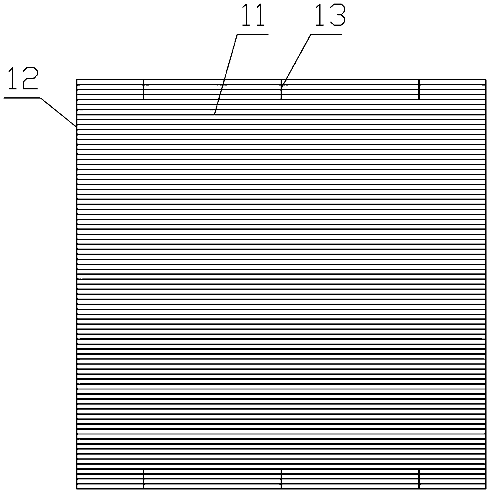
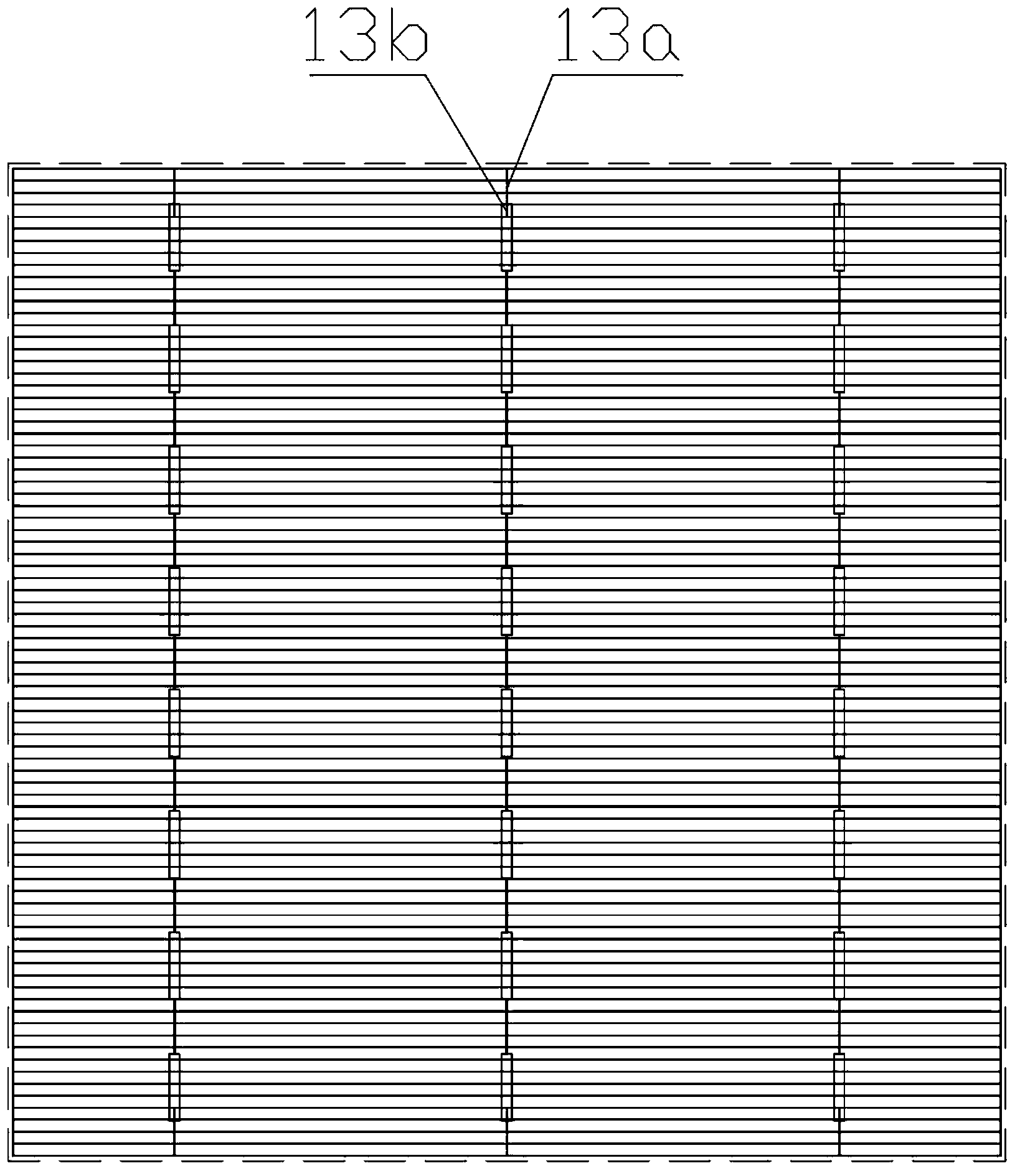
[0040] refer to Figure 1 to Figure 3 . The size of the polysilicon wafer is 156mm×156mm, Φ220mm. There are 3 main grid lines 20, the first sub-gate lines 11 and the second sub-gate lines 12 have a width of 50 μm, the third sub-gate lines 13 are 6, and the width is 180 μm, and the third sub-gate lines 13 are embedded The length of the portion 13b is 2 mm.
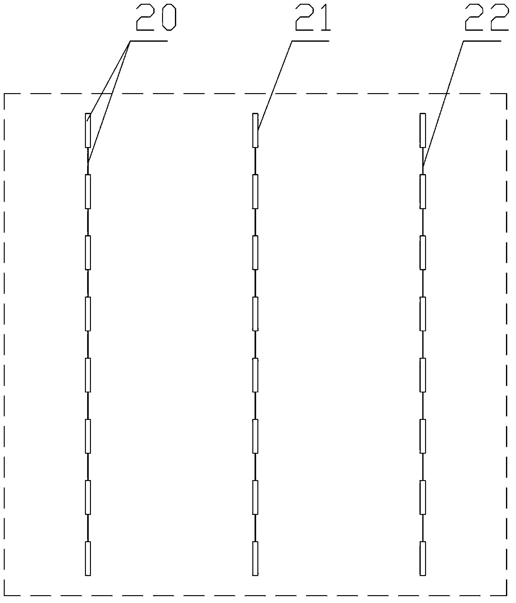
[0041] Each busbar 20 is composed of 8 rectangular sections 21 and 7 connecting lines 22 , the rectangular section 21 has a width of 1.6 mm and a length of 10.5 mm, and the connecting lines 22 have a length of 8.5 mm and a width of 150 μm.
[0042] After the above structural design of the front grid line electrode structure of the polysilicon wafer, the silver paste in the 20 part of the main grid line can be saved by 42%, and the light-receiving area is also increased at the same time.
[0043] After the polysilicon wafers that have been textured, diffused, etched, and coated are printed in the first and second passes, ...
Embodiment 2
[0045] refer to Figure 4 to Figure 6 . The size of single crystal silicon wafer is 125mm×125mm, Φ165mm. There are two main gate lines 20, the first sub-gate lines 11 and the second sub-gate lines 12 have a width of 50 μm, the third sub-gate lines 13 are four, and the width is 220 μm, and the third sub-gate lines 13 are embedded The length of segment 13b is 1.5 mm.
[0046] Each busbar 20 is composed of 6 rectangular sections 21 and 5 connecting lines 22. The rectangular section 21 has a width of 1.6 mm and a length of 11 mm, and the connecting line 22 has a length of 9 mm and a width of 150 μm.
[0047] After the above structural design of the front grid line electrode structure of the polysilicon wafer, the silver paste in the 20 part of the main grid line can be saved by 43.2%, and the light receiving area can also be increased at the same time.
[0048] After the first and second printing of the polysilicon wafer after texturing, diffusion, etching and coating, the Fi...
PUM
 Abstract
Description
Claims
Application Information
 - R&D Engineer
- R&D Manager
- IP Professional
- Industry Leading Data Capabilities
- Powerful AI technology
- Patent DNA Extraction
Browse by: Latest US Patents, China's latest patents, Technical Efficacy Thesaurus, Application Domain, Technology Topic, Popular Technical Reports.
© 2024 PatSnap. All rights reserved.Legal|Privacy policy|Modern Slavery Act Transparency Statement|Sitemap|About US| Contact US: help@patsnap.com


