
Electro static discharge protective circuit for circuit board interface

An electrostatic discharge protection, electrostatic discharge protection technology, applied in the field of electrostatic protection of circuit boards, can solve problems such as difficult protection ability, large TVS area, and difficulty in meeting the design requirements of radio frequency interfaces

Inactive Publication Date: 2012-11-07
BEIJING ZHONGKE XINWEITE SCI & TECH DEV +2
View PDF8 Cites 10 Cited by
  • Summary
  • Abstract
  • Description
  • Claims
  • Application Information

AI Technical Summary

Problems solved by technology

[0003] The technical problem to be solved by the present invention is to provide a circuit for electrostatic discharge protection of the circuit board interface, to overcome the problem that the TVS area is very large in the prior art and cannot reduce the parasitic capacitance of the TVS, and to use between the signal line and VDD, In the scheme of installing diodes between GND and signal lines, it is difficult to effectively combine the improvement of interface ESD protection capability with the reduction of interface parasitic capacitance, and it is difficult to meet the ESD design requirements of radio frequency interfaces.

Method used


Image

  • Electro static discharge protective circuit for circuit board interface
  • Electro static discharge protective circuit for circuit board interface
  • Electro static discharge protective circuit for circuit board interface

Examples


Embodiment Construction

[0041] The principles and features of the present invention are described below in conjunction with the accompanying drawings, and the examples given are only used to explain the present invention, and are not intended to limit the scope of the present invention.

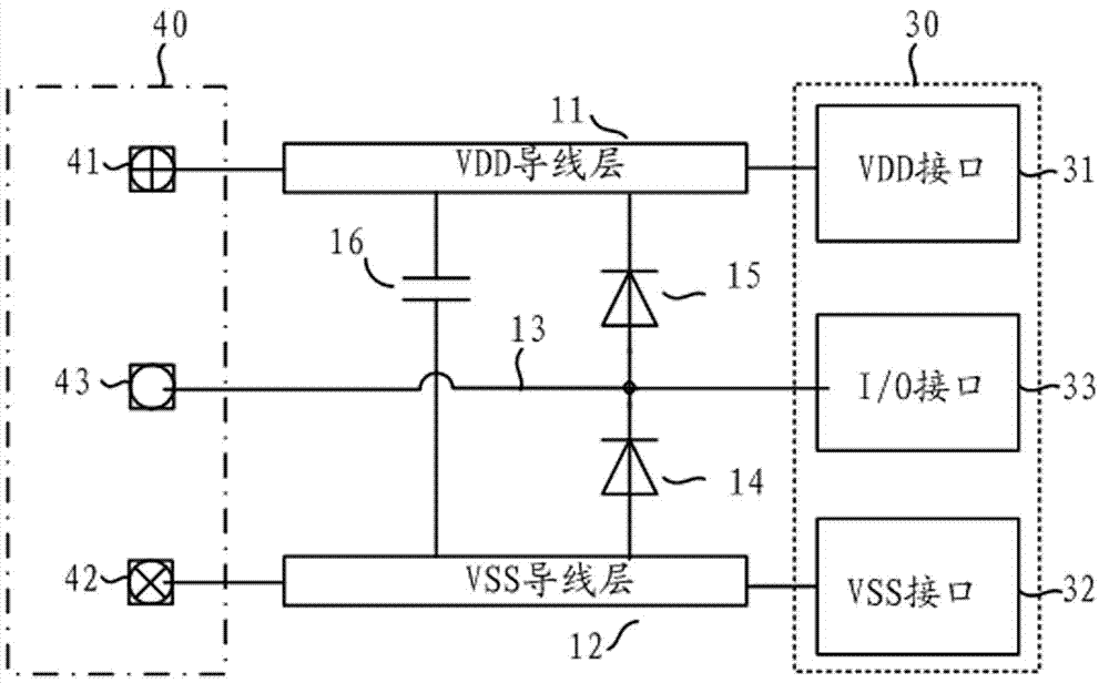
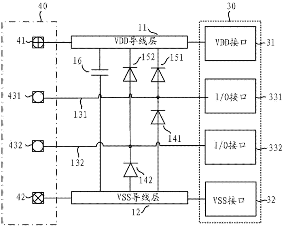
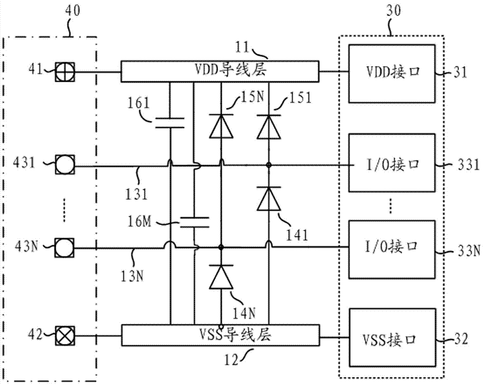
[0042] Such as figure 1 As shown, the circuit board interface electrostatic discharge protection circuit of the present invention includes a high-voltage wire layer 11 and a low-voltage wire layer 12; a capacitor 16 is electrically connected between the high-voltage wire layer and the low-voltage wire layer; the signal interface 33 (I / O interface) and The signal terminal 43 of the protected circuit 40 is connected together through the signal line 13; between the signal line 13 and the high voltage conductor layer 11, there is provided a first diode 15 whose polarity is forward biased from the signal line 13 to the high voltage conductor layer 11, That is, the anode of the first diode 15 is connected to the signal li...


PUM


Abstract

The invention relates to an electro static discharge protective circuit for a circuit board interface, which comprises a high voltage conductor layer, a low voltage conductor layer and a protected circuit with a signal interface. The protected circuit is electrically connected between the high voltage conductor layer and the low voltage conductor layer. An electro static storage circuit is arranged between the high voltage conductor layer and the low voltage conductor layer. A first diode circuit is arranged between the high voltage conductor layer and the signal interface, the positive pole end of the first diode circuit is connected with the signal interface, and the negative pole end of the first diode circuit is connected with the high voltage conductor layer. A second diode circuit is arranged between the low voltage conductor layer and the signal interface, the negative pole end of the second diode circuit is connected with the signal interface, and the positive pole end of the second diode circuit is connected with the low voltage conductor layer. When an electrostatic discharge event occurs at an external interface circuit, electrostatic charges are transmitted to the conductor layers through the diode circuits and are absorbed by the electrostatic storage circuit between the conductor layers, and the absorbed charges are released in the ways of protected circuit leakage and the like, thereby achieving the purpose of electrostatically protecting the protected circuit.

Description

technical field [0001] The invention relates to electrostatic protection of circuit boards, in particular to a circuit board interface electrostatic discharge protection circuit. Background technique [0002] Electro Static Discharge (ESD) protection technology is a key technology for the industrialization of integrated circuits and electronic equipment. According to reports, the damage to integrated circuits caused by electrostatic discharge accounts for 35% to 55% of the total damage to integrated circuits. ESD problems have cost nearly $30 billion. With the rapid development of communication technology, the interface with higher transmission speed has become an important factor restricting high-speed communication technology. Since the interface needs to be in frequent contact with the outside world in various environments, the ESD protection performance of the interface is usually required to reach the ESD HBM model (Human Body Model, Human Body Model) protection level ...

Claims


Application Information

Patent Timeline
IPC IPC(8): H02H9/04
Inventor 曾传滨海潮和李晶李多力罗家俊韩郑生
Owner BEIJING ZHONGKE XINWEITE SCI & TECH DEV
Learn More