Cyanide based electrolytic gold plating solution and plating method using same
A technology of cyanide alloy and conductive salt, which is applied in the field of cyanide-based electrolytic gold plating baths, can solve problems such as inability to perform cathodic current plating, and achieve the effects of excellent liquid stability, increased productivity, and shortened plating time
- Summary
- Abstract
- Description
- Claims
- Application Information
AI Technical Summary
Problems solved by technology
Method used
Image
Examples
Embodiment 1
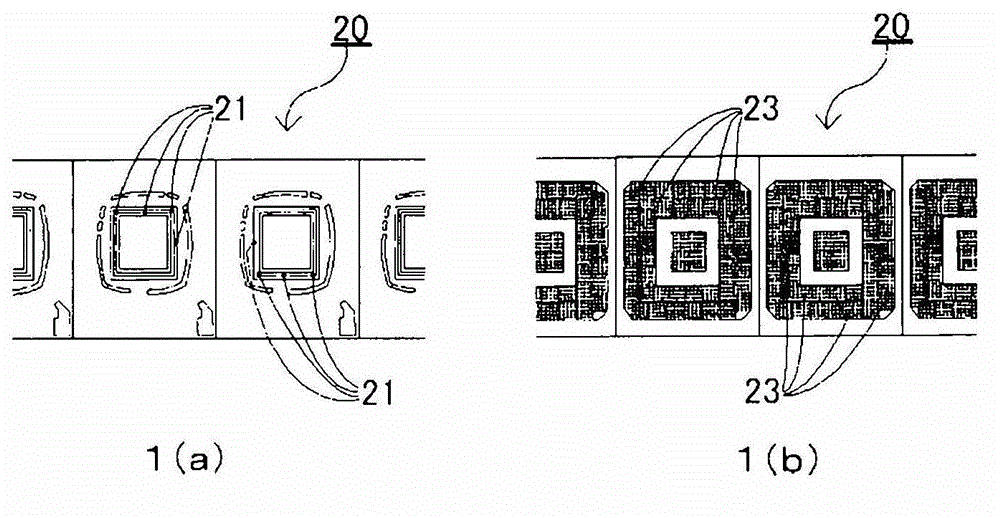
[0091] Under the plating conditions shown in Table 2, gold plating films were respectively formed on the samples and the BGA panel using a plating bath having the following composition.
[0092]
[0093] The film thickness of the obtained gold-plated film was 0.70-0.75 micrometers, and it was a uniform semi-glossy shape. As shown in Table 2, the cathode current density is 0.05~0.4A / dm 2Within the range of the cathode current efficiency, film thickness deviation, lead pull test and solder ball shear test results are good.
[0094] (Table 2)
[0095]
Embodiment 2
[0103] Under the plating conditions shown in Table 4, gold plating films were respectively formed on the samples and the BGA panel using a plating bath having the following composition.
[0104]
[0105] The film thickness of the obtained gold-plated film was 0.70-0.75 micrometers, and it was a uniform semi-glossy shape. As shown in Table 4, the cathode current density is 0.05~0.4A / dm 2 Within the range of the cathode current efficiency, film thickness deviation, lead pull test and solder ball shear test results are good.
[0106] (Table 4)
[0107]
Embodiment 3
[0109] Under the plating conditions shown in Table 5, gold-plated films were formed on the samples and the BGA panel, respectively, using a plating bath having the following composition.
[0110]
[0111]
[0112] The film thickness of the obtained gold-plated film was 0.70-0.75 micrometers, and it was a uniform semi-glossy shape. As shown in Table 5, the cathode current density is 0.05~0.4A / dm 2 Within the range of the cathode current efficiency, film thickness deviation, lead pull test and solder ball shear test results are good.
[0113] (table 5)
[0114]
PUM
| Property | Measurement | Unit |
|---|---|---|
| Cathode current density | aaaaa | aaaaa |
| Film thickness | aaaaa | aaaaa |
| Cathode current density | aaaaa | aaaaa |
Abstract
Description
Claims
Application Information
 - Generate Ideas
- Intellectual Property
- Life Sciences
- Materials
- Tech Scout
- Unparalleled Data Quality
- Higher Quality Content
- 60% Fewer Hallucinations
Browse by: Latest US Patents, China's latest patents, Technical Efficacy Thesaurus, Application Domain, Technology Topic, Popular Technical Reports.
© 2025 PatSnap. All rights reserved.Legal|Privacy policy|Modern Slavery Act Transparency Statement|Sitemap|About US| Contact US: help@patsnap.com


