In Gan/Si dual-junction solar cell

A solar cell, p-inxga1-xn technology, applied in the field of solar cells, can solve the problems of reducing the total conversion efficiency of the cell, increasing the complexity of the epitaxy process, increasing the production cost, etc., so as to improve the total conversion efficiency, improve the radiation resistance, The effect of prolonging the service life

Active Publication Date: 2012-10-24
TIANJIN LANTIAN SOLAR TECH +2
View PDF6 Cites 4 Cited by
  • Summary
  • Abstract
  • Description
  • Claims
  • Application Information

AI Technical Summary

Problems solved by technology

[0005] The patents retrieved above all use Si as the substrate to prepare InGaN solar cells, which solves the problems of lattice mismatch and thermal expansion

Method used


Image

  • In Gan/Si dual-junction solar cell
  • In Gan/Si dual-junction solar cell

Examples


Embodiment

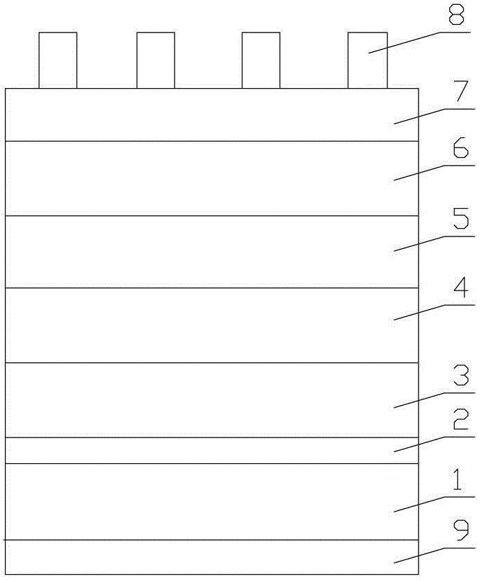
[0024] Embodiment: refer to attached Figure 1-Figure 2 , the fabrication process of the InGaN / Si double-junction solar cell of the present invention is described:

[0025] Step 1, select n-Si after ultrasonic cleaning as the substrate;

[0026] Step 2. Using Metal Organic Chemical Vapor Deposition (MOCVD), place the n-Si substrate 1 in the reaction chamber, and feed TMAl with a flow rate of 30mL / min and NH 3 The flow rate is 3L / min, and at 600°C, Al atoms begin to diffuse into the n-Si layer to replace Si atoms, forming a highly doped surface, and then the temperature rises to 1000°C, Al atoms diffuse further, forming a deep junction with the n-Si substrate 0.1um p-Si layer 2, on which a 60nm-thick AlN nucleation layer 3 grows; the p-Si layer and n-Si layer constitute a Si bottom battery, which is not only easy to prepare, but also a battery The total conversion efficiency can reach more than 30%;

[0027] Step 3, using metal-organic chemical vapor deposition technology to...


PUM

PropertyMeasurementUnit
Depthaaaaaaaaaa

Abstract

The invention relates to an In Gan/Si dual-junction solar cell which comprises an n-Si lining. An A1N nucleation layer, a GaN damping layer, an n-InxGa1-x layer, a p-InxGa1-xN layer and a positive electrode are sequentially arranged on the solar cell. The solar cell is characterized in that a p-Si layer is arranged between the nucleation layer and the lining and forms a Si-lining cell together with the n-Si lining, a semi-transparent current expansion layer is evaporated on the p-InxGa1-xN layer, and a negative electrode is evaporated below the n-Si lining. Since the p-Si layer is formed between the A1N nucleation layer and the n-Si lining and forms the Si-lining cell together with the n-Si lining, the solar cell is easy to manufacture and high in total conversion efficiency. By the aid of the evaporated semi-transparent current expansion layer, the solar cell is strong in radioresistance capacity and long in service life. Since the negative electrode is evaporated below the n-Si lining, process is simplified, cost is lowered, the solar cell can be used as a reflecting mirror, and the total conversion efficiency is improved.

Description

technical field [0001] The invention belongs to the technical field of solar cells, in particular to an InGaN / Si double-junction solar cell. Background technique [0002] At present, the known energy sources are non-renewable. After years of mining, the reserves of these energy sources are decreasing day by day, and they will cause serious environmental problems after use. More and more attention has been paid to the exhausted green energy. For a long time, we have been tirelessly looking for materials with high conversion efficiency of solar energy. In recent years, the third-generation semiconductor materials represented by GaN, InGaN, and AlGaN—group III nitrides have become a research hotspot. They are mainly used in optoelectronic devices and high-temperature, high-frequency, and high-power devices. The research results in 2002 showed that the forbidden band width of InN was not 1.89eV as previously reported but 0.7eV, which means that by adjusting the In composition i...

Claims


Application Information

Patent Timeline
IPC IPC(8): H01L31/0687H01L31/0224
CPCY02E10/50Y02E10/544Y02P70/50
Inventor 张启明王帅高鹏王保民刘如彬孙强穆杰
Owner TIANJIN LANTIAN SOLAR TECH
Why Eureka
Try Eureka