Coaxial through-silicon via
A through-silicon via and coaxial technology, applied in the field of semiconductor structures and their manufacturing, can solve problems such as inability to use
- Summary
- Abstract
- Description
- Claims
- Application Information
AI Technical Summary
Problems solved by technology
Method used
Image
Examples
Embodiment Construction
[0030] The accompanying drawings, which are incorporated in and constitute a part of this specification, illustrate the presently preferred embodiments of the invention, and the general description given above and the detailed description of the preferred embodiments given below serve to explain the principles of the invention.
[0031] It should be understood that, for simplicity and clarity of illustration, elements shown in the figures have not necessarily been drawn to scale. For example, the dimensions of some of the elements may be exaggerated relative to other elements for clarity.
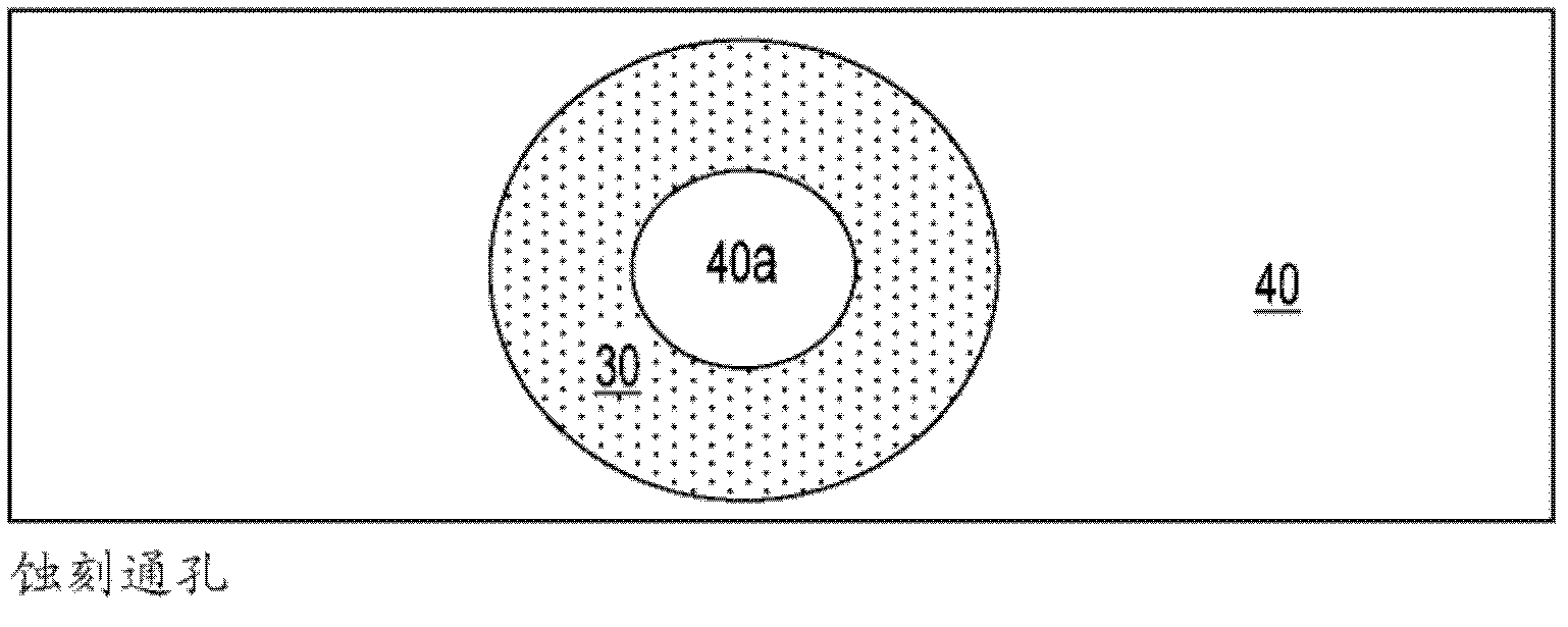
[0032] figure 2 A top view of an annular via 30 etched in a silicon substrate 40 is shown. For the sake of clarity, the structured active layer 45 is not shown in the plan view. The structure is provided with a central pillar 40a defined by etching, made of the same material as the substrate. The width of the central pillar is of the order of 6 μm.
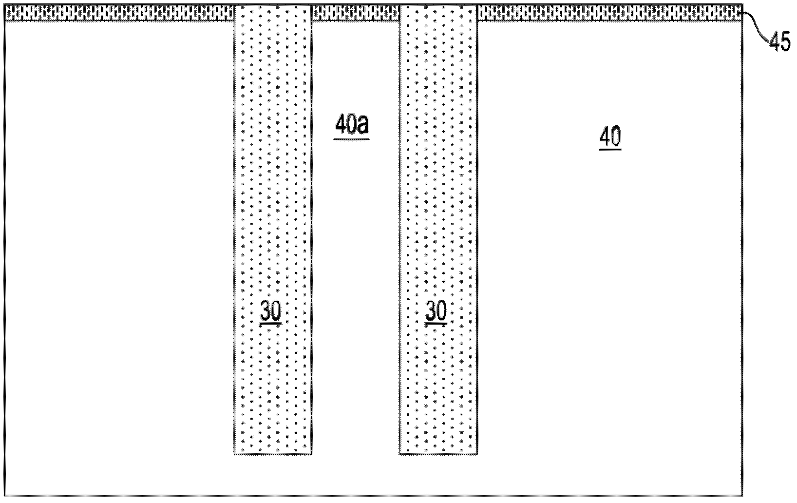
[0033] image 3 yes figure 2 , sho...
PUM
 Abstract
Description
Claims
Application Information
 - R&D
- Intellectual Property
- Life Sciences
- Materials
- Tech Scout
- Unparalleled Data Quality
- Higher Quality Content
- 60% Fewer Hallucinations
Browse by: Latest US Patents, China's latest patents, Technical Efficacy Thesaurus, Application Domain, Technology Topic, Popular Technical Reports.
© 2025 PatSnap. All rights reserved.Legal|Privacy policy|Modern Slavery Act Transparency Statement|Sitemap|About US| Contact US: help@patsnap.com


