
Wafer detecting apparatus

A detection device and wafer technology, which is applied to measurement devices, optical devices, instruments, etc., can solve the problems of complex structure, difficult to detect error slot state, difficult to implement, etc.

Active Publication Date: 2012-07-11
SHINKO ELECTRIC CO LTD
View PDF7 Cites 15 Cited by
  • Summary
  • Abstract
  • Description
  • Claims
  • Application Information

AI Technical Summary

Problems solved by technology

[0013] Also, as a second bad case, such as Figure 12 As shown, for example, among the two stacked wafers W1 and W2, the upper wafer W1 moves further to the front side than the lower wafer W2 due to vibrations when the lid (not shown) of the wafer storage container is opened. In the state of moving (the cover side), the light from the illumination device 100 can be irradiated onto the end surface T1 of the upper wafer W1, but the light from the illumination device 100 cannot be illuminated because the front part of the upper wafer W1 is blocked. The light is irradiated onto the lower side of the end face T2 of the wafer W2
As a result, the overlapping state cannot be detected
[0014] Also, as a third undesirable case, such as Figure 13 As shown, since the illumination light source (not shown) located in the inspection head K is configured to irradiate light from the front of the wafer W in the XA direction, it cannot illuminate from the XB direction and the XC direction on the left and right sides of the wafer W. Light
Therefore, the range that can be imaged by the imaging device (not shown) located in the inspection head K is a narrow range near the center of the wafer W in the left-right direction, so it is easily affected by local contamination of the wafer W, etc. And it is difficult to detect error slot state
In addition, although it is also possible to Figure 13 Move the illumination light source and the imaging device in the left and right directions and take pictures of the wafer at multiple positions in the left and right directions, so as to reliably detect the state of the error groove, but this not only makes the overall structure of the device complicated, but also prolongs the detection time, making it difficult to implement.

Method used


Image

  • Wafer detecting apparatus
  • Wafer detecting apparatus
  • Wafer detecting apparatus

Examples


Embodiment Construction

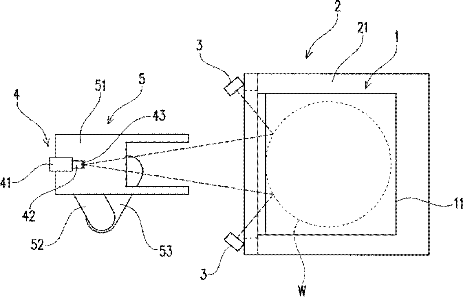
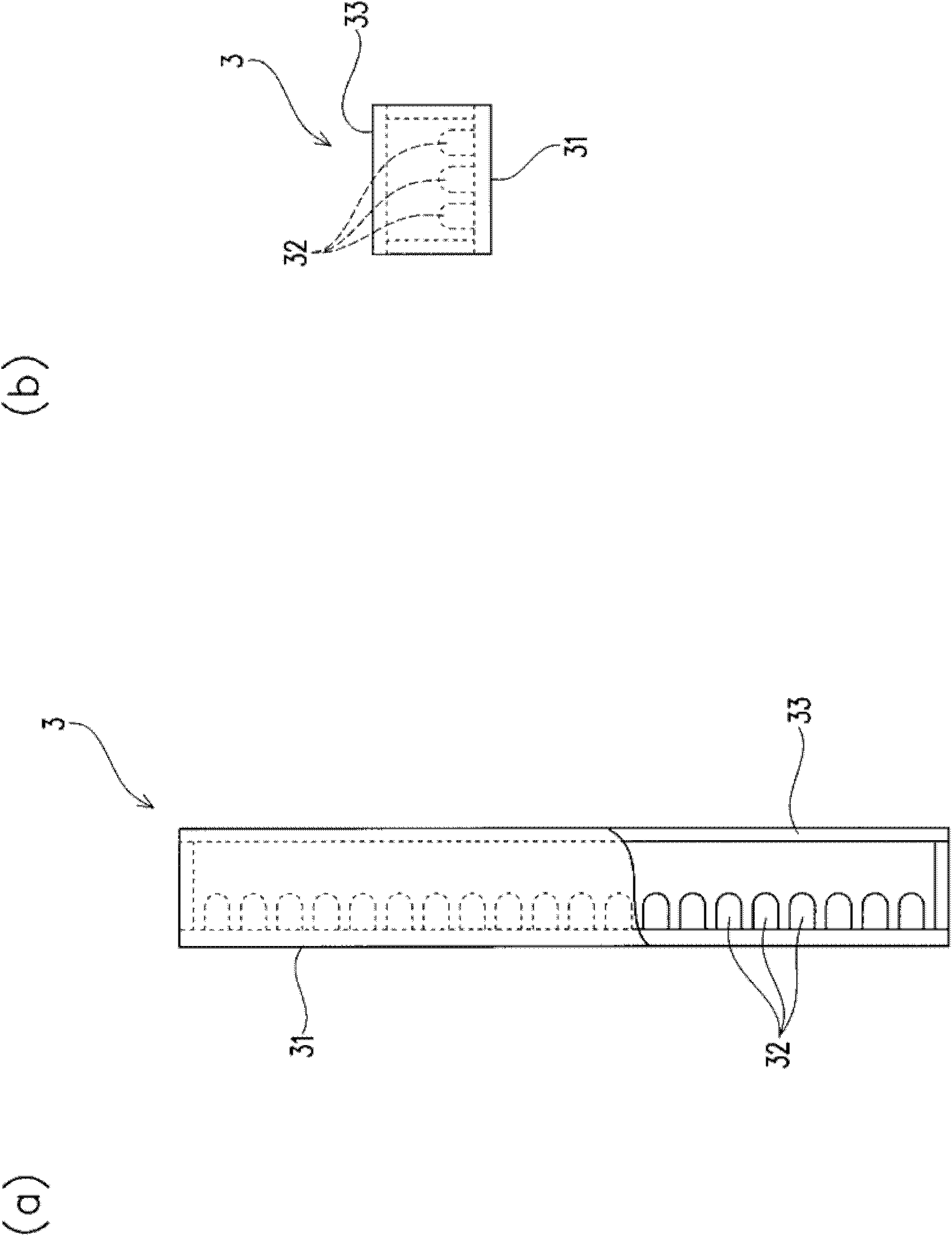
[0036] figure 1 and figure 2 The wafer inspection device of this embodiment is shown. The wafer inspection device has lighting devices 3, 3 and an imaging device 4, and the lighting devices 3, 3 are arranged on the left and right sides of the loading port 2 for loading the wafer container 1 for The wafer W is accommodated; the light from the illuminating devices 3 and 3 is irradiated on the end face of the wafer W, and the reflected light from the end face is incident on the camera 4, and the camera 4 is used to take pictures of the end face. In this way, by using the reflective wafer inspection device, it is possible to detect the wafer without causing any problems even if the wafer is warped or warped.

[0037] The above-mentioned wafer storage container 1 has a casing 11 opened at the front, and a plurality of slots 12 for stacking and storing wafers W in the casing 11 at predetermined intervals in the vertical direction (refer to Figure 5 (a)) and a cover 13 for clos...


PUM


Abstract

Disclosed is a wafer detecting apparatus which can accurately detect a wafer storage state. The wafer detecting apparatus detects the storage state of a plurality of wafers (W) in a wafer storing container (1), which is capable of storing the wafers by stacking the wafers in the vertical direction and is capable of having the wafers carried in and out from the front. The wafer detecting apparatus is provided with: a long illuminating apparatus (3), which irradiates the wafers in the wafer container (1) with light, and which is long in the vertical direction; and an image pickup apparatus (4) having reflected light inputted thereto, said reflected light being the light emitted from the illuminating apparatus (3), applied to the wafers (W) and reflected. The image pickup apparatus (4) is disposed on the front side of the wafer storing container (1), and the illuminating apparatus (3) is disposed on the left and / or the right side of the image pickup apparatus (4).

Description

technical field [0001] The present invention relates to a wafer detection device for detecting the storage state of wafers accommodated in a wafer storage container for accommodating a plurality of wafers. Background technique [0002] Conventionally, there has been used a wafer container that accommodates a plurality of wafers in slots located inside the wafer container, and that accommodates the wafers through an opening at the front of the wafer container. The circle enters and exits the wafer holding container. [0003] Such a wafer container is transported by a robot or the like, and placed on an opening and closing device (hereinafter referred to as a loading port) for opening and closing the lid of the wafer container. The port is, for example, an additional device mounted on a wafer processing device or the like for performing predetermined processing on a wafer. [0004] However, the storage state of the wafer in the wafer storage container has the following three...

Claims


Application Information

Patent Timeline
Patent Type & Authority Applications(China)
IPC IPC(8): H01L21/67G01B11/00
CPCH01L21/67265G01B11/00H01L21/67
Inventor 安田克己神垣敏雄溝河巧
Owner SHINKO ELECTRIC CO LTD
Learn More