Device structure conducive to eliminating U-shaped nickel silicide and corresponding technology thereof
A technology of nickel silicide and device structure, which can be used in semiconductor devices, semiconductor/solid-state device manufacturing, electrical components, etc., and can solve problems such as voids and chamfers
- Summary
- Abstract
- Description
- Claims
- Application Information
AI Technical Summary
Problems solved by technology
Method used
Image
Examples
Embodiment approach
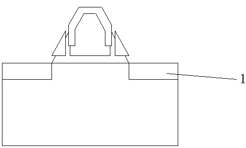
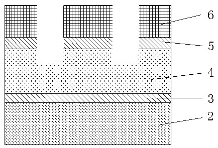
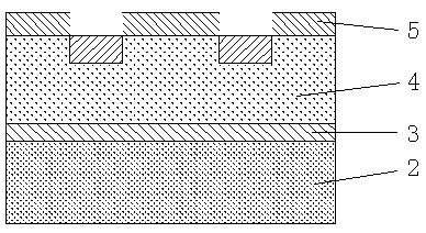
[0030] Please continue to see Figure 2 to Figure 4 shown. In the first step, thin film deposition is performed on polysilicon 4, and then photoresist is spin-coated, and then the silicon oxide layer is opened by dry etching. That is, through flim stack deposition + PR patterning + dry etching (oxide open) to achieve such as figure 2 It is shown with an oxide 5 and a PR layer 6 respectively on polysilicon 4 . In the second step, the photoresist layer 6 on the polysilicon 4 is removed, and then high-temperature oxidation treatment is performed. That is, through PR remove + oxidation to achieve such as image 3 The polysilicon 4 shown, and the photoresist layer 6 is removed. In the third step, the polysilicon gate is etched on the polysilicon 4, and then the oxide 5 is removed. That is, through normal poly etching + oxide strip to achieve such as Figure 4 Polysilicon 4 shown. By first molding the gate with a partially grooved top, a gate nickel silicide with a straight ...
PUM
 Abstract
Description
Claims
Application Information
 - R&D
- Intellectual Property
- Life Sciences
- Materials
- Tech Scout
- Unparalleled Data Quality
- Higher Quality Content
- 60% Fewer Hallucinations
Browse by: Latest US Patents, China's latest patents, Technical Efficacy Thesaurus, Application Domain, Technology Topic, Popular Technical Reports.
© 2025 PatSnap. All rights reserved.Legal|Privacy policy|Modern Slavery Act Transparency Statement|Sitemap|About US| Contact US: help@patsnap.com


