
RFID (radio frequency identification) tag chip

A technology of RFID tags and chips, applied in the field of radio frequency identification, can solve the problems of increased system complexity, high cost, complex structure, etc., and achieve the effect of low cost, high performance, and huge market prospects

Inactive Publication Date: 2012-06-27
颜力 +1
View PDF2 Cites 20 Cited by
  • Summary
  • Abstract
  • Description
  • Claims
  • Application Information

AI Technical Summary

Problems solved by technology

Semi-active electronic tags can have a long service life, will not cause electromagnetic pollution, and are less affected by the use environment; however, the structure of semi-active electronic tags is more complicated than active electronic tags, and the cost is also higher
[0004] At present, many application scenarios require the use of passive electronic tags, active electronic tags and semi-active electronic tags at the same time; for example, the confidential item management system requires electronic tags to be attached to confidential items such as paper documents, mobile storage devices, mobile phones, and cameras ; Passive electronic tags are used on paper documents, thin and portable; mobile storage devices, mobile phones and cameras contain a large number of metal parts, and semi-active electronic tags need to be used to improve reading performance; however, RFID tag chips on the market only support One kind of incentive mode, different air interface protocols used by RFID tag chips in different incentive modes, need to be used with their respective readers; therefore, if the existing RFID tag chip products on the market are used, paper documents and other Items are equipped with two sets of RFID systems, which use their own air interface protocols and readers to finally summarize the obtained data to the background processing, which increases the complexity of the system

Method used


Image

  • RFID (radio frequency identification) tag chip
  • RFID (radio frequency identification) tag chip
  • RFID (radio frequency identification) tag chip

Examples


Embodiment Construction

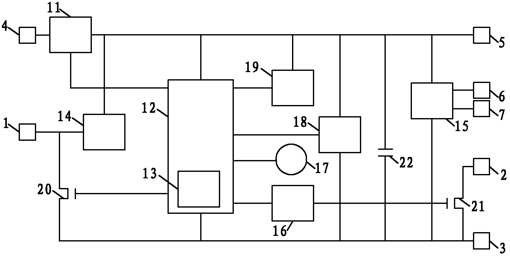
[0023] The present invention will be further described below in conjunction with drawings and embodiments.

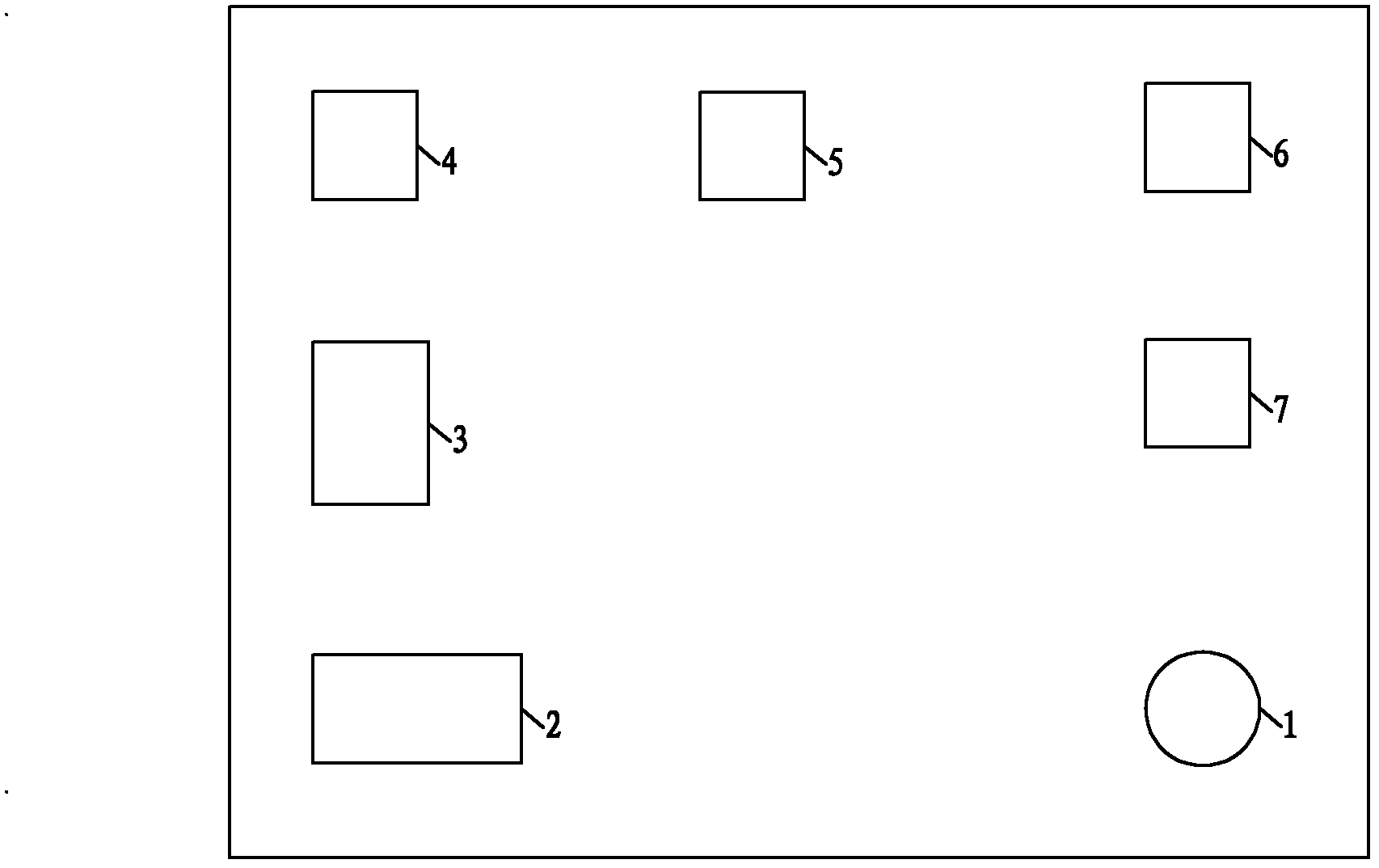
[0024] Please refer to figure 1 and figure 2 as shown, figure 1 It is a structural block diagram of the RFID tag chip of the present invention; figure 2 It is a schematic diagram of the bonding pad of the RFID tag chip of the present invention.

[0025]In this embodiment, an RFID tag chip includes: an excitation mode setting unit and a transceiver unit; the excitation mode setting unit includes seven pads, which are respectively the radiation antenna pin 1, the coupling antenna pin 2, and the negative pole of the power supply. Pin 3, external battery pin 4, power supply positive pin 5, first trigger coil pin 6 and second trigger coil pin 7; the transceiver unit includes: power control unit 11, logic unit 12, memory 13 , ultra-high frequency rectification unit 14, low frequency rectification unit 15, pulse generating unit 16, oscillator unit, parallel voltage regul...


PUM


Abstract

The invention discloses an RFID tag chip applied to the field of radio frequency identification, which comprises a motivation mode setting unit and a transceiver unit, wherein the motivation mode setting unit is used for setting a motivation mode of the chip into a passive mode, an active mode, a semi-active mode or a trigger mode; the transceiver unit is connected with the motivation mode setting unit and is used for flexibly selecting a connecting antenna, an externally-connecting battery or a trigger coil according to selected motivation mode, and modulating data inside the chip to a carrier wave to be emitted to a reader by converting a load impedance or a Q value of the antenna connected with the chip. According to the invention, the manufacturing costs of an active electronic tag or a semi-active electronic tag are reduced, and the requirements of application occasions of requiring the passive electronic tag, the active electronic tag or the semi-active electronic tag are satisfied.

Description

technical field [0001] The invention relates to the field of radio frequency identification, in particular to an RFID tag chip. Background technique [0002] RFID is radio frequency identification technology, also known as electronic tags and radio frequency identification, which can identify specific targets and read and write related data through radio signals without the need to establish mechanical or optical contact between the identification system and specific targets. The ultimate development goal of the Internet of Things is to install RFID tags for all people and objects, and use reader devices and network devices to obtain various information about people and objects anytime, anywhere. RFID tags contain RFID tag chips, tag antennas, and sometimes batteries. [0003] According to the different excitation methods of RFID tag chips, RFID tags can be divided into the following three categories: 1) Passive electronic tags. There is no battery in the passive electroni...

Claims


Application Information

Patent Timeline
Patent Type & Authority Applications(China)
IPC IPC(8): G06K19/077
Inventor 颜力王新华
Owner 颜力
Learn More