Boron nitride-graphene composite material, preparation method and purpose thereof
A composite material and graphene technology, which is applied in semiconductor/solid-state device manufacturing, electrical components, electrical solid-state devices, etc., can solve problems such as unsatisfactory electrical conductivity, and achieve the effect of improving electrical conductivity
- Summary
- Abstract
- Description
- Claims
- Application Information
AI Technical Summary
Problems solved by technology
Method used
Image
Examples
Embodiment 1
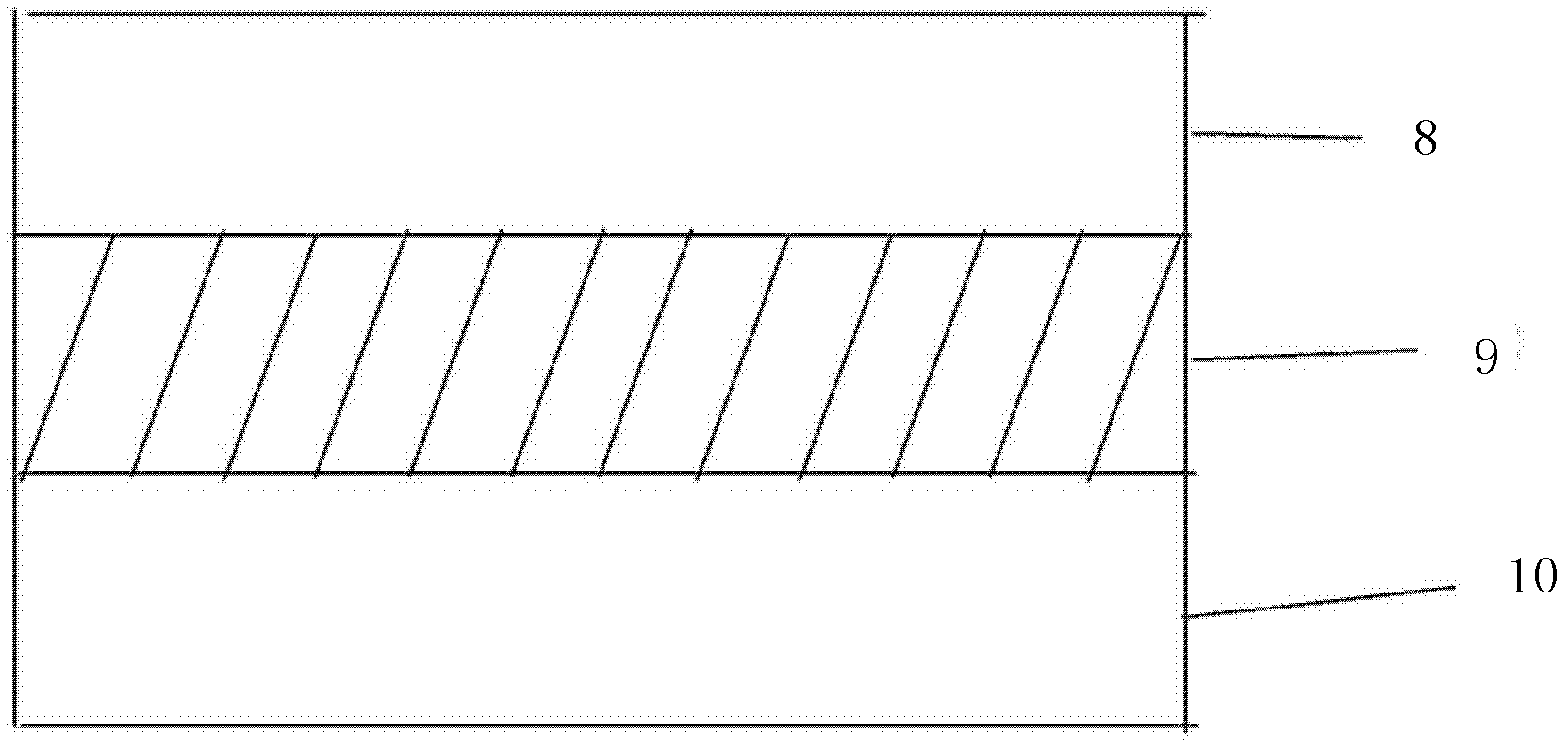
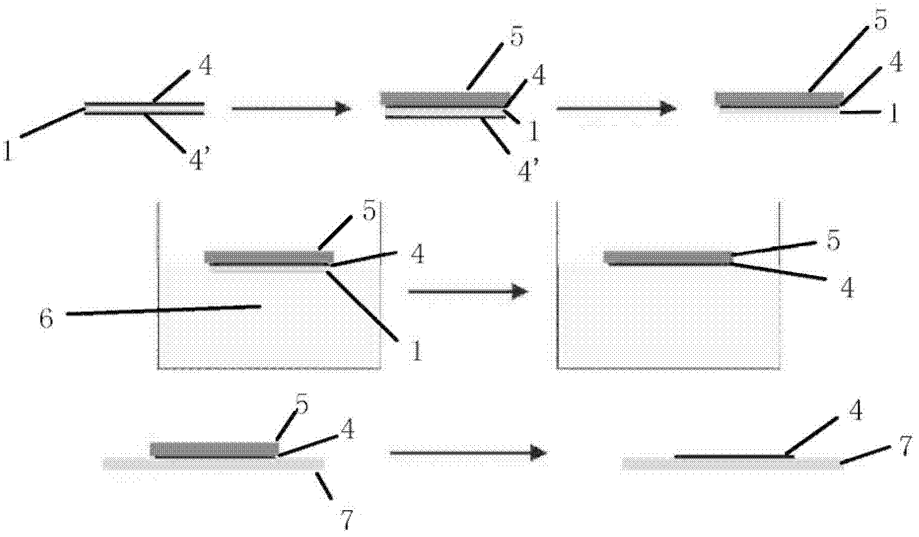
[0072] Two square boron nitride films (thickness 3nm, side length 5cm) and a single-layer graphene film of the same shape and size (thickness 0.35nm) were grown on the copper foil by the CVD method described in the text. PMMA glue was sprayed and cured on one surface of each of them, and the copper foil was exposed by plasma etching with oxygen on the other side, and the copper foil was etched away by immersing in a hydrochloric acid (20% by weight) solution. Then one of the boron nitride films is cleaned and put into the water. The boron nitride film is flat on the surface of the water due to surface tension, and it is picked up from the water with a glass substrate to make it flat and tightly attached to the surface of the water without gaps. The surface of the substrate; then the single-layer graphene film is cleaned and laid flat on the surface of the water, and the glass substrate coated with the boron nitride film is used to pick it up from the water and make it tightly a...
Embodiment 2
[0075] The boron nitride film / graphene film / boron nitride film composite material was prepared in the same manner as in Example 1, except that the thicknesses of the boron nitride film and the graphene film were 5 nm and 1 nm, respectively.
[0076] The plane resistance of the composite material was measured by the plane resistance measurement method with the aforementioned plane resistance measuring instrument, and the results are shown in Table 1 below.
Embodiment 3
[0078] The boron nitride film / graphene film / boron nitride film composite material was prepared in the same manner as in Example 1, except that the thicknesses of the boron nitride film and the graphene film were 0.5 nm and 3.5 nm, respectively.
[0079] The plane resistance of the composite material was measured by the plane resistance measurement method with the aforementioned plane resistance measuring instrument, and the results are shown in Table 1 below.
PUM
| Property | Measurement | Unit |
|---|---|---|
| Thickness | aaaaa | aaaaa |
| Thickness | aaaaa | aaaaa |
| Thickness | aaaaa | aaaaa |
Abstract
Description
Claims
Application Information
 - R&D
- Intellectual Property
- Life Sciences
- Materials
- Tech Scout
- Unparalleled Data Quality
- Higher Quality Content
- 60% Fewer Hallucinations
Browse by: Latest US Patents, China's latest patents, Technical Efficacy Thesaurus, Application Domain, Technology Topic, Popular Technical Reports.
© 2025 PatSnap. All rights reserved.Legal|Privacy policy|Modern Slavery Act Transparency Statement|Sitemap|About US| Contact US: help@patsnap.com


