OLED (Organic Light Emitting Diode) reticle, manufacturing method thereof and reflecting type sighting telescope

A manufacturing method and reticle technology, applied in telescopes, semiconductor/solid-state device manufacturing, instruments, etc., can solve the problems of high cost, difficulty in disassembly and assembly, space occupied by reticle and lighting system, etc., and achieve low cost, Great flexibility and space-saving effect

Active Publication Date: 2012-05-16
GUAN YEOLIGHT TECH CO LTD +1
View PDF3 Cites 4 Cited by
  • Summary
  • Abstract
  • Description
  • Claims
  • Application Information

AI Technical Summary

Problems solved by technology

[0004] 1. The reticle and lighting system take up a lot of space and are not easy to disassemble
[0005] 2. The aiming mark on the reticle cannot change color according to the target to be aimed at different distances
[0006] 3. The reticle is an imaging optical component, so the transparency and cleanliness of the reticle are highly required, so the cost is relatively high

Method used


Image

  • OLED (Organic Light Emitting Diode) reticle, manufacturing method thereof and reflecting type sighting telescope
  • OLED (Organic Light Emitting Diode) reticle, manufacturing method thereof and reflecting type sighting telescope
  • OLED (Organic Light Emitting Diode) reticle, manufacturing method thereof and reflecting type sighting telescope

Examples


Embodiment 1

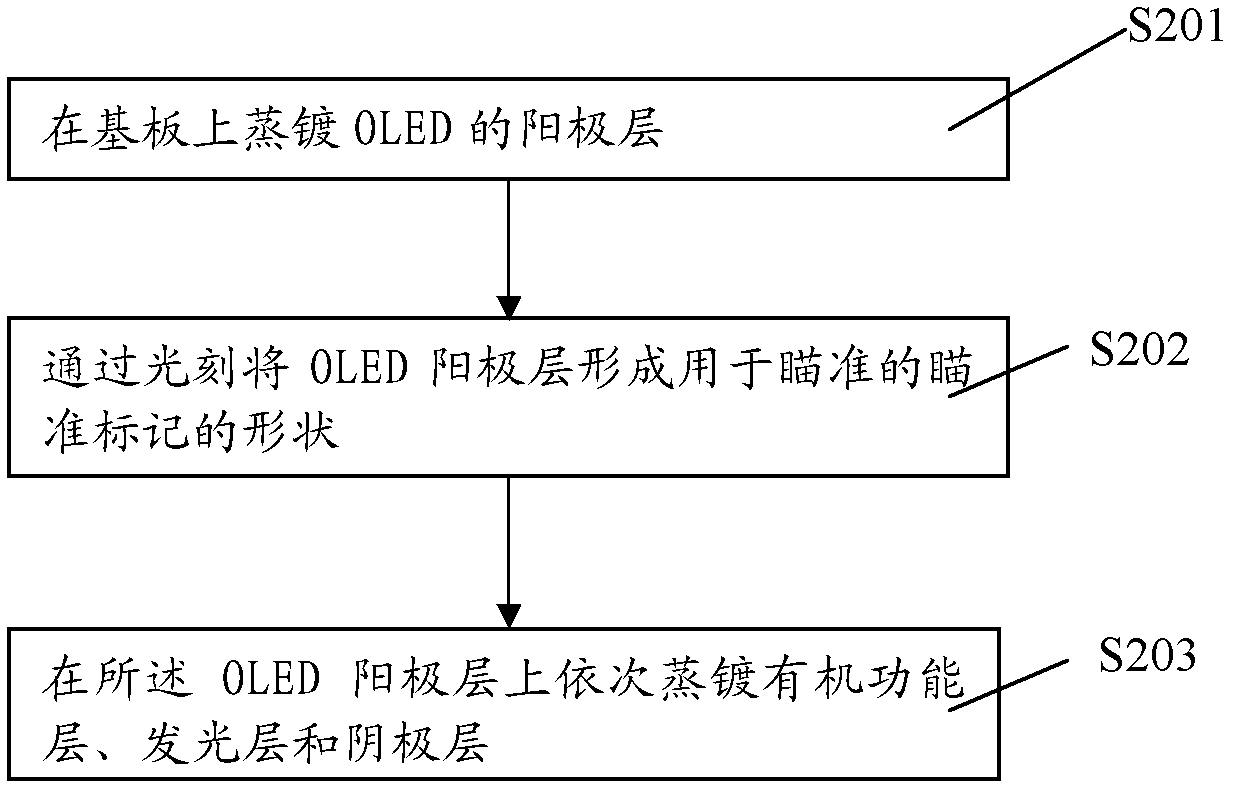
[0039] The OLED reticle of this embodiment of the present invention is made by the following method:

[0040] First, a layer of ITO conductive film is evaporated on the OLED substrate as the OLED anode layer;

[0041] Next, the ITO conductive film was formed into the shape of the aiming mark by photolithography, thereby forming the anode layer of the OLED in the shape of the aiming mark. Such as Figure 4 As shown, it gives the shape of the pattern of the aiming mark photoetched on the anode layer, wherein the circle is the shape of the lens (such as the shape of the lens of the reflex sight), and the shape of the pattern of the aiming mark includes the the graduated lines 11 and 12, the arrowed line 14, and the curve and the graduated line 13 in the area between the graduated line 11 and the arrowed line 14 on the radius of the circle;

[0042] Next, an organic functional layer, a light-emitting layer and a cathode layer are sequentially vapor-deposited on the OLED anode laye...

Embodiment 2

[0045] In this embodiment, the OLED anode layer of the OLED reticle is photoetched into the shape of a cross-shaped aiming mark, such as Figure 5 shown. Others are the same as in Example 1.

Embodiment 3

[0047] In this embodiment, the OLED anode layer of the OLED reticle is photoetched in the shape of an aiming mark with a cross and a small circular ring in the center of the cross, as Figure 6 shown. Others are the same as in Example 1.


PUM


Abstract

The invention provides a manufacturing method of an OLED (Organic Light Emitting Diode) reticle, comprising the following steps: evaporating an anode layer of an OLED on a substrate, and enabling the anode layer to form a sighted and marked shape; and sequentially evaporating an organic functional layer, a light emitting layer and a cathode layer on the anode layer of the OLED. The invention also provides an OLED reticle comprising the OLED, wherein the OLED comprises the substrate as well as the anode layer, the organic functional layer, the light emitting layer and the cathode layer which are sequentially overlapped on the substrate, wherein the anode layer of the OLED is in the sighted and marked shape. In addition, the invention provides a reflecting type sighting telescope with the OLED reticle provided by the invention. By using the OLED reticle, the manufacturing method thereof and the reflecting type sighting telescope, the space occupied by the reticle in the reflecting type sighting telescope and a lamp optical system can be greatly reduced.

Description

technical field [0001] The invention relates to a reflective sight (Reflex), in particular to an OLED reticle, a manufacturing method thereof, and a reflective sight using the OLED reticle. Background technique [0002] Existing reflex sights (Reflex), such as figure 1 As shown, it mainly includes a spectroscope 2 , a reticle 3 , and an illumination system 4 . The optical analysis mirror 2 is a semi-transparent and semi-reflective lens, one side of the lens is convex, and the other side is concave, and one or more optical analysis films are coated on the concave surface. The reticle 3 has a hollowed-out reticle pattern as an aiming mark. When the light emitted by the illumination system 4 illuminates the reticle 3, an aiming mark is formed on the optical analysis mirror 2 and reflected, and enters the human eye 5 with parallel light, and the human eye 5 can see an aiming mark located at infinity. Simultaneously, the human eye 5 also sees the target 1 to be aimed at a dist...

Claims


Application Information

Patent Timeline
Patent Type & Authority Applications(China)
IPC IPC(8): H01L51/56H01L51/52G02B27/34G02B23/00
Inventor 邱勇吴空物
Owner GUAN YEOLIGHT TECH CO LTD
Why Eureka
Try Eureka