Double-input direct-current converter using non-isolation type pulse voltage source unit
A DC converter and pulse voltage technology, which is applied in the direction of converting DC power input to DC power output, electrical components, adjusting electrical variables, etc. simple structure
- Summary
- Abstract
- Description
- Claims
- Application Information
AI Technical Summary
Problems solved by technology
Method used
Image
Examples
specific Embodiment 1
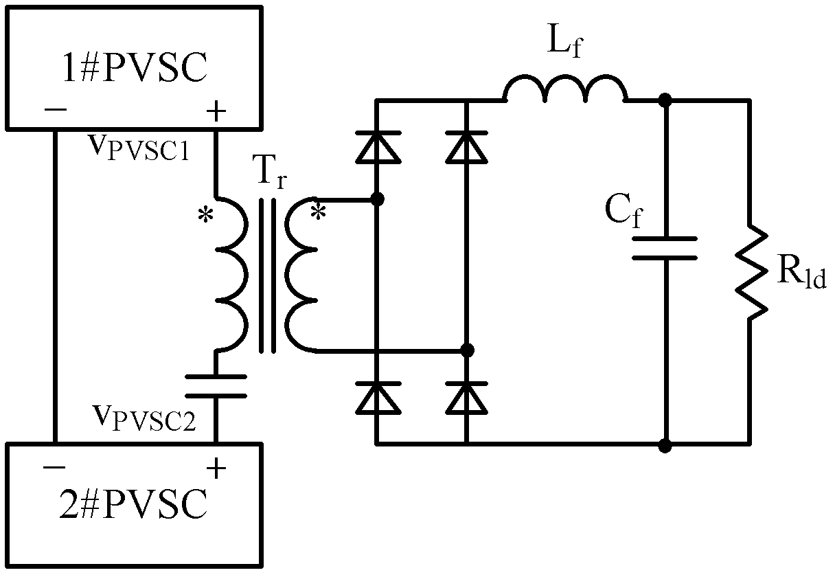
[0047] Such as image 3 The complete circuit diagram of the specific embodiment 1 shown, the dual-input DC converter includes: two non-isolated pulse voltage source units PVSC 1, PVSC 2, transformer T r, rectifier circuit, output filter circuit, load R Ld . Define two non-isolated pulse voltage source units PVSC 1 and PVSC 2 as 1# source and 2# source respectively, V in1 and V in2 is the input voltage of 1# source and 2# source, V in1 , Q 1 and Q 3 Form a buck PVSC, V in2 , Q 2 and Q 4 Form another buck PVSC. C 1 、C 2 、C 3 、C 4 for Q 1 , Q 2 , Q 3 , Q 4 The junction capacitance, D 1 、D 2 、D 3 、D 4 for Q 1 , Q 2 , Q 3 , Q 4 of the parasitic body diode. L r To add a resonant inductance to realize the zero-voltage switching of the switching tube, C b is the blocking capacitor. D. R1 、D R2 is the transformer T r Secondary rectifier diode, L f is the filter inductance, C f is the filter capacitor.
[0048] Specific Embodiment 1 There are two wo...
specific Embodiment 2
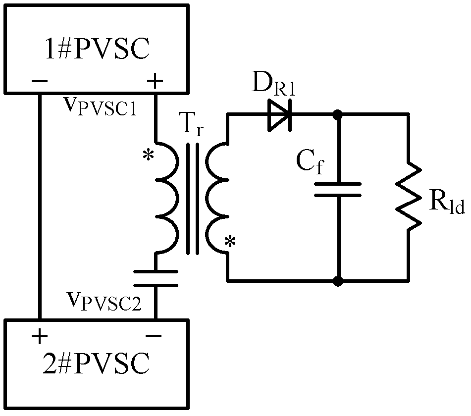
[0074] Such as Figure 6 The complete circuit diagram of specific embodiment 2 is shown. , the dual-input DC converter includes: two non-isolated pulse voltage source units PVSC 1, PVSC 2, transformer T r, rectifier circuit, output filter circuit, load R Ld . Define two non-isolated pulse voltage source units PVSC 1 and PVSC 2 as 1# source and 2# source respectively, V in1 and V in2 is the input voltage of 1# source and 2# source, V in1 , Q 1 and Q 3 Form a buck PVSC, V in2 , Q 2 and Q 4 Form another buck PVSC. C 1 ~C 4 for Q 1 ~Q 4 The junction capacitance, D 1 ~D 4 for Q 1 ~Q 4 of the parasitic body diode. L r To add a resonant inductance to realize the zero-voltage switching of the switching tube, C b is the DC blocking capacitor, L m for the transformer T r Primary side magnetizing inductance. D. R is the transformer T r Secondary rectifier diode, C f is the filter capacitor.
[0075] The specific embodiment 2 also has two working modes accordi...
PUM
 Abstract
Description
Claims
Application Information
 - R&D
- Intellectual Property
- Life Sciences
- Materials
- Tech Scout
- Unparalleled Data Quality
- Higher Quality Content
- 60% Fewer Hallucinations
Browse by: Latest US Patents, China's latest patents, Technical Efficacy Thesaurus, Application Domain, Technology Topic, Popular Technical Reports.
© 2025 PatSnap. All rights reserved.Legal|Privacy policy|Modern Slavery Act Transparency Statement|Sitemap|About US| Contact US: help@patsnap.com


