Semiconductor wet etching device and method

A wet etching, semiconductor technology, applied in semiconductor/solid-state device manufacturing, electrical components, circuits, etc., can solve problems such as uneven corrosion, inability to corrode silicon wafers, film residues, etc., to increase the vertical corrosion rate and increase flow Sexuality, the effect of reducing residue

Inactive Publication Date: 2012-04-18
HANGZHOU LION MICROELECTRONICS CO LTD
View PDF5 Cites 0 Cited by
  • Summary
  • Abstract
  • Description
  • Claims
  • Application Information

AI Technical Summary

Problems solved by technology

[0002] The current mainstream wet etching method adopts the method of immersing the wafer in the etching solution. For some difficult-to-etch substances, it cannot give a better etching effect on the silicon wafer, especially for thicker films and Residue and uneven etch are often seen in mixed material films

Method used


Image

  • Semiconductor wet etching device and method
  • Semiconductor wet etching device and method

Examples


Embodiment Construction

[0018] Below in conjunction with accompanying drawing, the present invention will be further described:

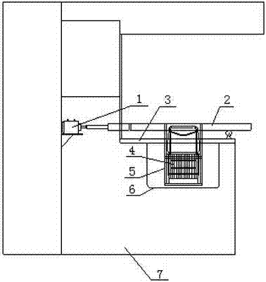
[0019] A device for semiconductor wet etching, including an equipment support 7, on which a transmission device, a flower basket support 5 and a tank body 6 containing corrosive liquid are arranged, and the transmission device drives the flower basket support 5 to reciprocate in the tank body 6.

[0020] Specifically, the transmission device is composed of a cylinder 1, a guide rail bracket 2 and a guide rail 3. The cylinder 1 is fixedly arranged on the inside of the equipment support 7, and is connected to the guide rail bracket 2 that is arranged on the outside of the equipment support 7 through a transmission shaft. Slidingly arranged on the guide rail 3, the guide rail 3 is arranged on the side edge above the tank body 6; a pulley can be set on the guide rail 3, and the guide rail bracket 2 can slide on the pulley to realize reciprocating motion; the flower basket brack...


PUM


Abstract

The invention belongs to the field of manufacturing of semiconductor devices and particularly discloses a semiconductor wet etching device and a semiconductor wet etching method. The device is characterized in that: an equipment bracket is provided with a transmission device, a basket bracket and a tank body for accommodating an etching solution in a matched mode, wherein the transmission device drives the basket bracket to reciprocate in the tank body. Due to a mode of swinging back and forth, a basket for accommodating wafers has a larger motion track, so that liquidity of the etching solution is improved, impact kinetic energy of the etching solution on an etching body is provided by controlling back-and-forth swinging amplitude and frequency when liquidity of a chemical etching solution is improved, and a longitudinal etching rate of the etching solution can be effectively improved; therefore, the etching uniformity is improved, and the residue of the etching body is reduced.

Description

technical field [0001] The invention belongs to the field of semiconductor device manufacturing, in particular to a semiconductor wet etching device and method. Background technique [0002] The current mainstream wet etching method adopts the method of immersing the wafer in the etching solution. For some difficult-to-etch substances, it cannot give a better etching effect on the silicon wafer, especially for thicker films and Mixed material films often exhibit residue and inhomogeneous corrosion. Contents of the invention [0003] Aiming at the problems existing in the prior art, the object of the present invention is to provide a technical solution of a semiconductor wet etching device and method. [0004] The semiconductor wet etching device includes an equipment support, which is characterized in that a transmission device, a flower basket support and a tank body containing corrosive liquid are arranged on the equipment support, and the transmission device drives the...

Claims


Application Information

Patent Timeline
Patent Type & Authority Applications(China)
IPC IPC(8): H01L21/67
Inventor 陈宝华郑振宇王海峰周诗雨朱灵辉朱春生黄力平
Owner HANGZHOU LION MICROELECTRONICS CO LTD
Why Eureka
Try Eureka