Gate drive circuit unit, gate drive circuit and display device
A technology of gate drive circuit and holding circuit, which is applied in the field of gate drive circuit and display device, can solve the problem of strict limitation of drive circuit area, and achieve the effects of saving area, simplifying structure, and utilizing area
- Summary
- Abstract
- Description
- Claims
- Application Information
AI Technical Summary
Problems solved by technology
Method used
Image

Examples
Embodiment 1
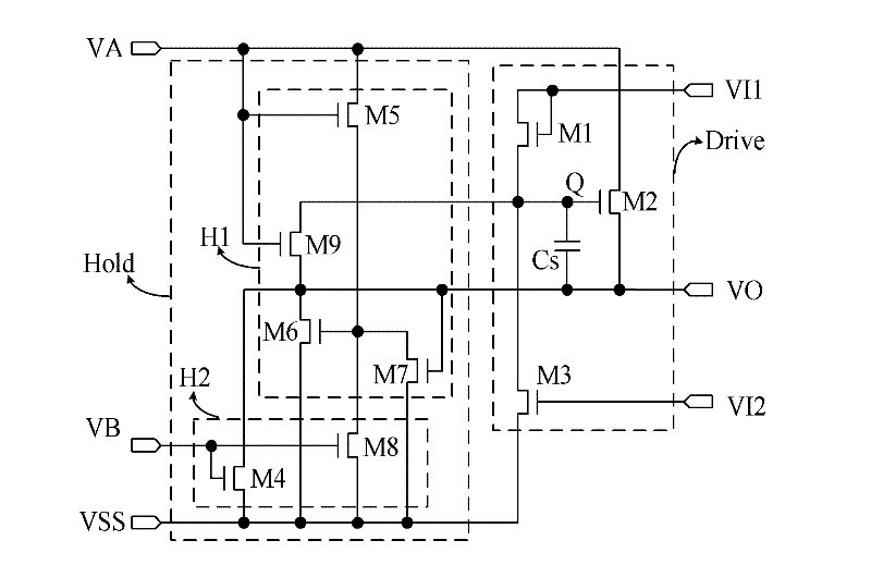
[0044] see figure 1 as shown, figure 1 As a gate driving circuit unit provided by an embodiment of the present invention, the first embodiment of the present invention starts from delaying the input signal of VI2. When the signal output by the output terminal of the circuit unit is transmitted to the subsequent circuit unit through the grid line load of the pixel area in the panel, the input signal of the second signal input terminal VI2 of the latter circuit unit is higher than that of the output terminal VO of the previous circuit unit. The output signal has a time delay, which can delay the release of the Q-point charge. The gate drive circuit unit includes:
[0045] Two signal input terminals, the first signal input terminal VI1 and the second signal input terminal VI2;
[0046] Two clock signal input terminals, the first clock signal input terminal VA and the second clock signal input terminal VB, the two clock signal input terminals input two columns of square wave cl...
Embodiment 2
[0087] Please refer to Image 6 , Image 6 It is a schematic diagram of the gate driving circuit unit of the second embodiment of the present invention. Compared with the gate drive circuit unit circuit of the first embodiment of the present invention, the unit circuit of the second embodiment adjusts the structure of the drive part (Drive): a third clock signal input terminal VC is added, and the transistor in the first embodiment is M3 is coupled to the source of the common ground terminal VSS, and is changed to be coupled to the third clock signal input terminal VC. The clock signal input by the third clock signal input terminal VC has twice the frequency of the signals input by the first clock signal input terminal VA and the second clock signal input terminal VB, that is, the period of the third clock signal is the period of the first clock signal 1 / 2 of. The purpose of this embodiment is still to delay the drop of the potential of the node Q of the unit circuit, and u...
no. 1 example 1
[0088] Please refer to Figure 7 , a timing diagram of the gate driving circuit unit according to the second embodiment of the present invention. Like the first embodiment, the working sequence of the unit circuit of the gate driving circuit of the second embodiment is also divided into two major stages: a driving stage (Driving) and a holding stage (Holding). Likewise, the two major stages can be subdivided into five smaller stages. To avoid repetition, only the working principle of the t3 stage of the driving stage (Driving) will be described in detail. In the stage t3, a low-level signal is input to the first clock signal input terminal VA of the unit circuit, and a high-level signal is input to the second clock signal input terminal VB. The second signal input terminal VI2 inputs a high-level signal to turn on the transistor M3, and before the input signal of the third clock signal input terminal VC jumps from high level to low level, the potential of node Q remains at a...
PUM
 Abstract
Description
Claims
Application Information
 - R&D
- Intellectual Property
- Life Sciences
- Materials
- Tech Scout
- Unparalleled Data Quality
- Higher Quality Content
- 60% Fewer Hallucinations
Browse by: Latest US Patents, China's latest patents, Technical Efficacy Thesaurus, Application Domain, Technology Topic, Popular Technical Reports.
© 2025 PatSnap. All rights reserved.Legal|Privacy policy|Modern Slavery Act Transparency Statement|Sitemap|About US| Contact US: help@patsnap.com