Laser assisted device alteration using two-photon absorption

一种激光束、激光源的技术,应用在缺陷分析领域,能够解决高峰值电源等问题,达到高缺陷定位、高分辨率的效果

Active Publication Date: 2012-04-04
DCG SYST
View PDF4 Cites 7 Cited by
  • Summary
  • Abstract
  • Description
  • Claims
  • Application Information

AI Technical Summary

Problems solved by technology

However, it requires higher peak power and pulsed beams so that the probability of two photons arriving at exactly the same time is greatly increased

Method used


Image

  • Laser assisted device alteration using two-photon absorption
  • Laser assisted device alteration using two-photon absorption
  • Laser assisted device alteration using two-photon absorption

Examples


Embodiment Construction

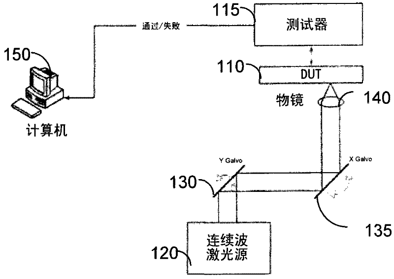
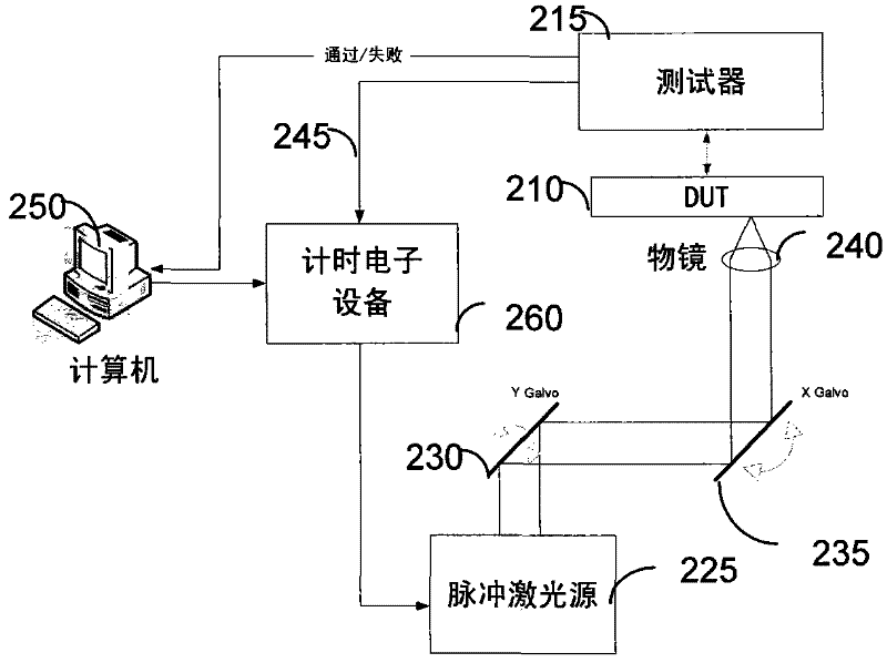
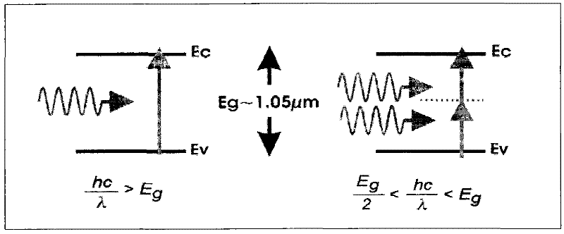
[0019] The embodiment of the present invention utilizes LADA technology to accurately inject carriers into the IC by applying two-photon absorption (TPA) to realize defect localization. To generate TPA, embodiments of the present invention use a femtosecond pulsed laser of appropriate energy. The technique is based on two photons arriving simultaneously at a focal point in a transistor such that the total energy of the photons is greater than that required to generate an electron-hole pair. Two-photon excitation requires excitation using femtosecond laser pulses with photon energies smaller than the bandgap of the semiconductor under test. More specifically, the incident laser photon energy is precisely set to be equal to or greater than half the material's bandgap. Because two-photon absorption is quadratically proportional to peak intensity, the signal is strongly localized to the laser focus, with direct improvements in defect localization and image resolution over single-...


PUM


Abstract

A Two-Photon Laser Assisted Device Alteration technique is presented. Fault localization is investigated by exploiting the non-linear two-photon absorption mechanism to induce LADA effects. Femtosecond laser pulses of wavelength having photon energy lower than the silicon band gap are directed at the area of interest, while the DUT is stimulated with test vectors. The laser pulses are synchronized to the DUT stimulation, so that switching timing can be altered using the two-photon absorption effect.

Description

[0001] related application [0002] This application claims priority to US Provisional Patent Application No. 61 / 381023 filed on September 8, 2010, the entire disclosure of which is incorporated herein by reference. technical field [0003] The present invention relates to the field of laser-based defect localization analysis of integrated circuits, and, more particularly, to the field of design debugging and / or defect analysis of integrated circuits using laser irradiation. Background technique [0004] Laser Assisted Device Alteration (LADA) is a technique applied to the test and debug phase of chip design. It is especially used to isolate critical performance-limiting nodes in complex, defect-free integrated circuits. It has also been found that the LADA effect is widely used to locate process defects because it tends to tune the characteristics of transistors in the same way as process defects. [0005] LADA technology is based on the ability of continuous wave (CW) la...

Claims


Application Information

Patent Timeline
Patent Type & Authority Applications(China)
IPC IPC(8): G01B11/00H01S3/11
CPCG01R31/303G01R31/311G01N21/63G01N21/636
Inventor P·韦达加尔巴D·里德
Owner DCG SYST
Why Eureka
Try Eureka