Manufacturing method of photovoltaic device and solar cell

A solar cell and manufacturing method technology, applied in photovoltaic power generation, final product manufacturing, energy conversion devices, etc., can solve problems such as low production capacity, photovoltaic cell surface damage, etc., and achieve simplified manufacturing, high-accuracy patterning, and easy manufacturing processes. Effect

Active Publication Date: 2014-06-04
TAIWAN SEMICON MFG CO LTD
View PDF6 Cites 0 Cited by
  • Summary
  • Abstract
  • Description
  • Claims
  • Application Information

AI Technical Summary

Problems solved by technology

These methods have been found to cause low yield and damage to the surface of photovoltaic cells
Therefore, although the existing methods can generally achieve the desired purpose, they are not satisfactory in all aspects.

Method used


Image

  • Manufacturing method of photovoltaic device and solar cell
  • Manufacturing method of photovoltaic device and solar cell
  • Manufacturing method of photovoltaic device and solar cell

Examples


Embodiment Construction

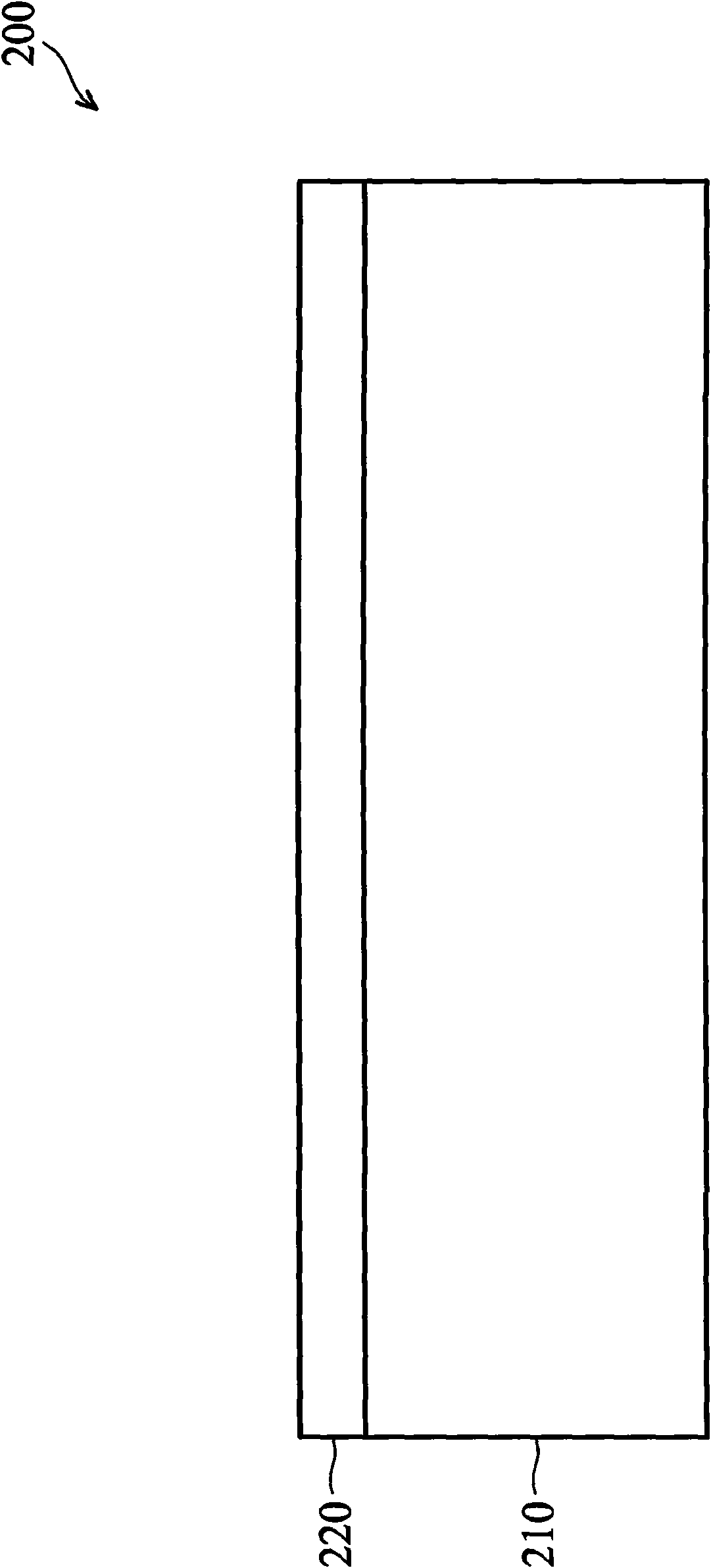
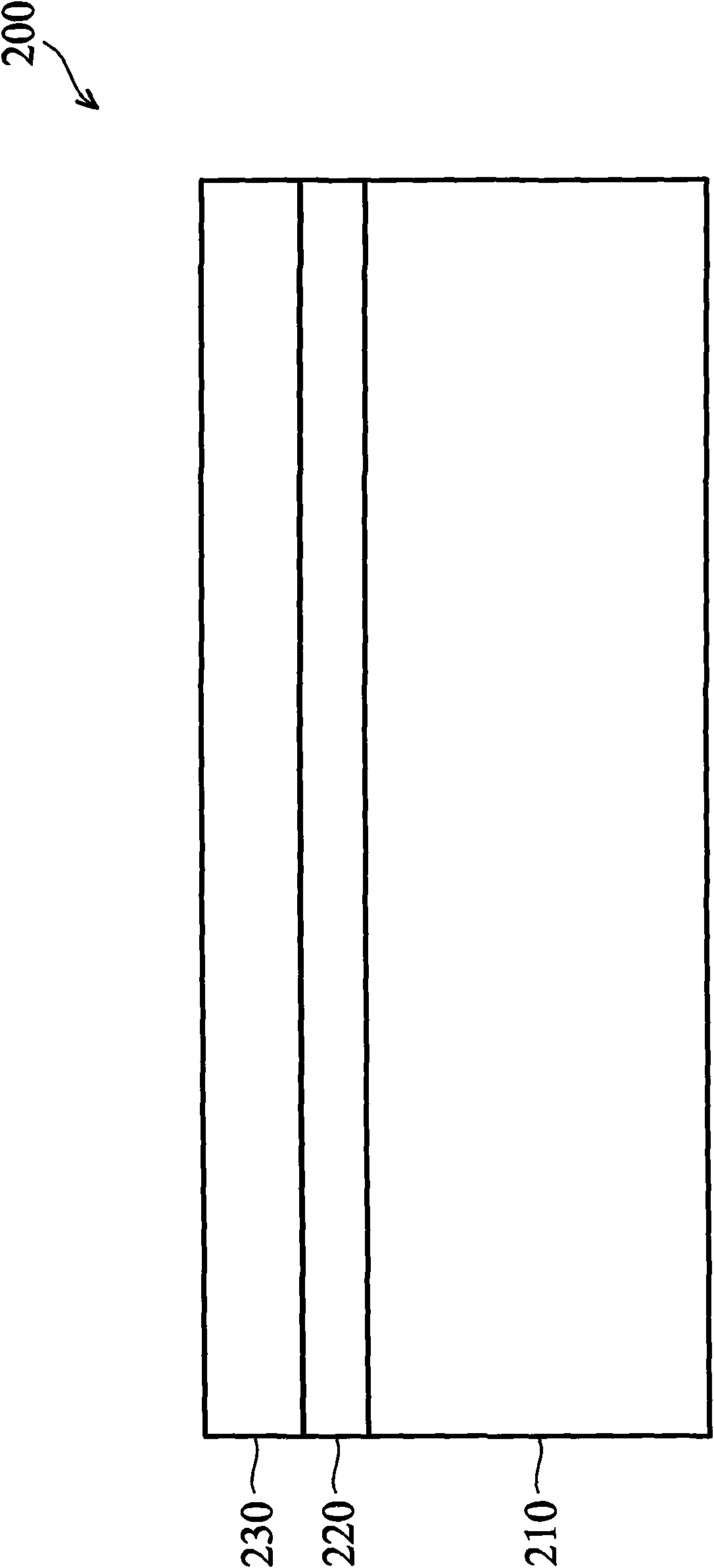
[0029] A number of different embodiments are provided due to different features of the invention. The specific elements and arrangements in the present invention are for simplicity, but the present invention is not limited to these embodiments. For example, a description of forming a first element on a second element may include embodiments in which the first element is in direct contact with the second element as well as embodiments having additional elements formed between the first element and the second element such that the second element An embodiment in which one element is not in direct contact with a second element. In addition, the present invention is represented by repeated symbols and / or letters in different examples for the sake of simplification and clarity, but does not indicate the relationship between the various embodiments and / or structures.

[0030] Traditionally, photovoltaic devices have been fabricated using laser or mechanical dicing to define, wire, ...


PUM


Abstract

A photovoltaic device manufacturing method is disclosed. Methods include manufacturing a photovoltaic cell using nanoimprint technology to define individual cell units of the photovoltaic device. The methods can include providing a substrate; forming a first conductive layer over the substrate; forming first grooves in the first conductive layer using a nanoimprint and etching process; forming an absorption layer over the first conductive layer, the absorption layer filling in the first grooves; forming second grooves in the absorption layer using a nanoimprint process; forming a second conductive layer over the absorption layer, the second conductive layer filling in the second grooves; and forming third grooves in the second conductive layer and the absorption layer, thereby defining a photovoltaic cell unit.

Description

technical field [0001] The invention relates to a photovoltaic cell, in particular to the preparation of a photovoltaic cell. Background technique [0002] Photovoltaic cells, also known as solar cells, convert light energy into electricity. In order to provide a higher conversion rate, the industry continues to develop photovoltaic cells and their fabrication methods. For example, thin film photovoltaic cells have provided better conversion efficiency. Traditionally, thin-film photovoltaic devices are prepared by using laser and mechanical cutting to define, wire, and isolate photovoltaic devices to form individual connected photovoltaic cells. These methods have been found to cause low productivity and damage to the surface of the photovoltaic cell. Therefore, although the existing methods can generally achieve the desired purpose, they are not satisfactory in all aspects. Contents of the invention [0003] In order to overcome the disadvantages of the prior art, the...

Claims


Application Information

Patent Timeline
Patent Type & Authority Patents(China)
IPC IPC(8): H01L31/18
CPCH01L31/0749H01L27/1425Y02E10/541H01L31/18H01L31/022425H01L31/03923H01L31/03928H01L31/0463Y02P70/50H01L31/04
Inventor 涂志强陈俊郎
Owner TAIWAN SEMICON MFG CO LTD
Why Eureka
Try Eureka