
Patsnap Eureka
For R&D, Patsnap Eureka makes reading and utilizing patents & technical documents easy.
Patsnap Eureka AIR
Designed for self-driven R&D workflows. Generate viable solutions, solve complex R&D challenges, empower your innovation with AI.

Patsnap Eureka Materials
Designed for material experts only. Revolutionize your material R&D, from search, analyze, to developing new materials.

TechResearch
Generate reliable direction feasibility study reports for your R&D in just a few steps.

TechSeek
Discover and master advanced knowledge NOW. Basics, ideas, possibilities, all at once.

TechMind
As an expert in R&D Theories, TechMind can generates customized viable solutions instantly.

TechRisk
Analyze your overall solution with one click, know your potential R&D risks in advance.

TechMonitor
Get weekly tech updates, stay abreast of the latest tech innovations and key insights.
Display panel module assembly device
A technology for display panels and assembly devices, which can be used in transportation and packaging, furnaces, electrical components, etc., and can solve problems such as the overall length of the device
- Summary
- Abstract
- Description
- Claims
- Application Information
AI Technical Summary
Problems solved by technology
Method used
Image

Examples
Embodiment 1
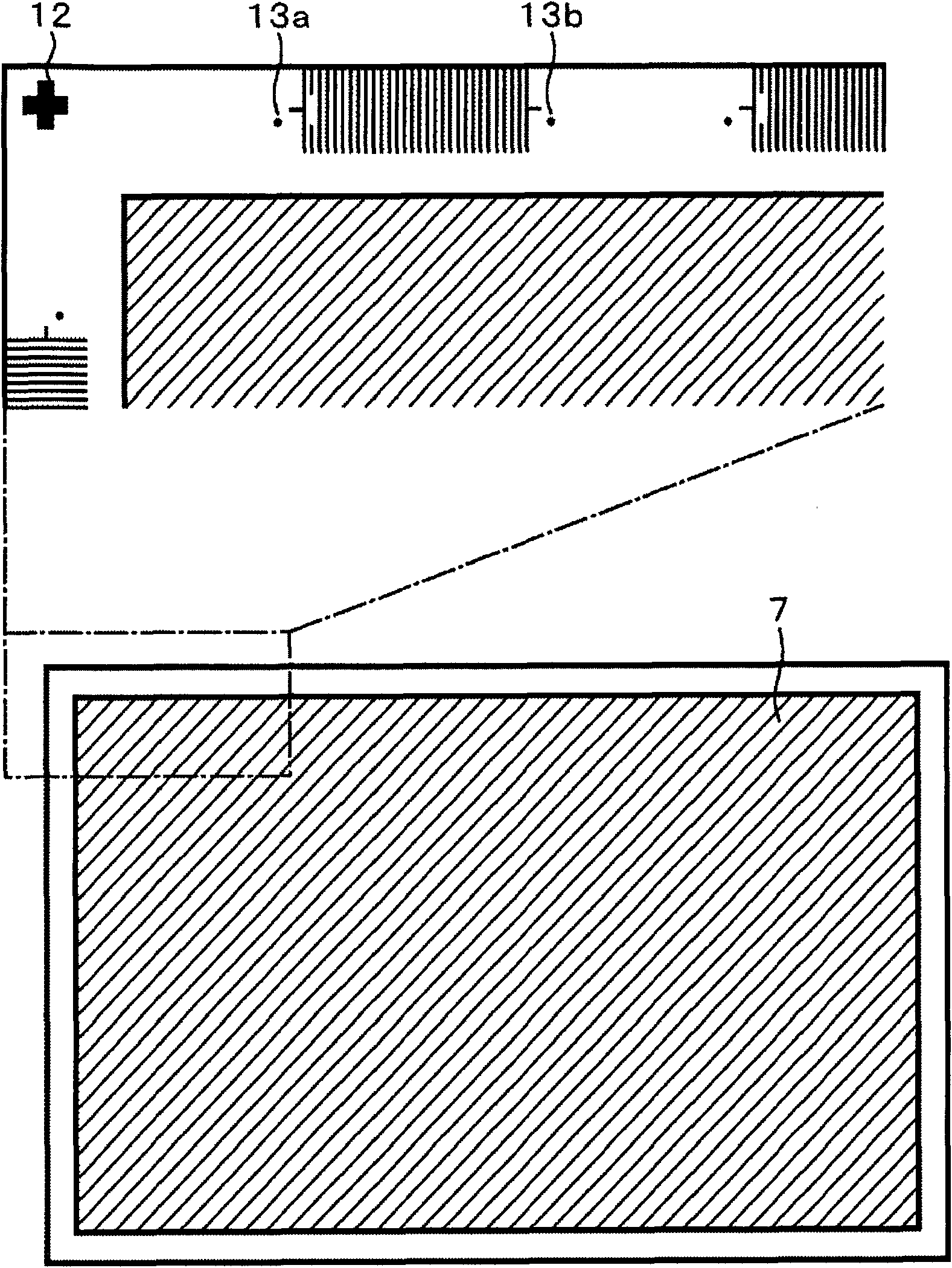
[0127] First, the assembly process of the display panel module will be briefly described. Figure 13 It is a figure for demonstrating the assembly process of a display panel module. The assembly of the display panel module is carried out as follows.
[0128] (a) Terminal cleaning step: a step of cleaning the peripheral terminal region of the display panel substrate 7 . Wipe and remove (45) foreign matter and the like at the terminal portion with a cleaning tape 44 dipped in a solvent or the like. As other foreign matter removal methods, methods using UV and plasma may also be employed.
[0129] (b) ACF pasting step (panel side): a step of pasting the anisotropic conductive film (ACF) on the display panel substrate 7 . The ACF 46 is softened and temporarily attached ( 47 ) to the device mounting position of the display panel substrate 7 at a temperature ranging from several tens of degrees Celsius or less to around 100 degrees Celsius.
[0130] (c) Mounting step: a step of ...
Embodiment 2
[0218] Next, Example 2 will be described.
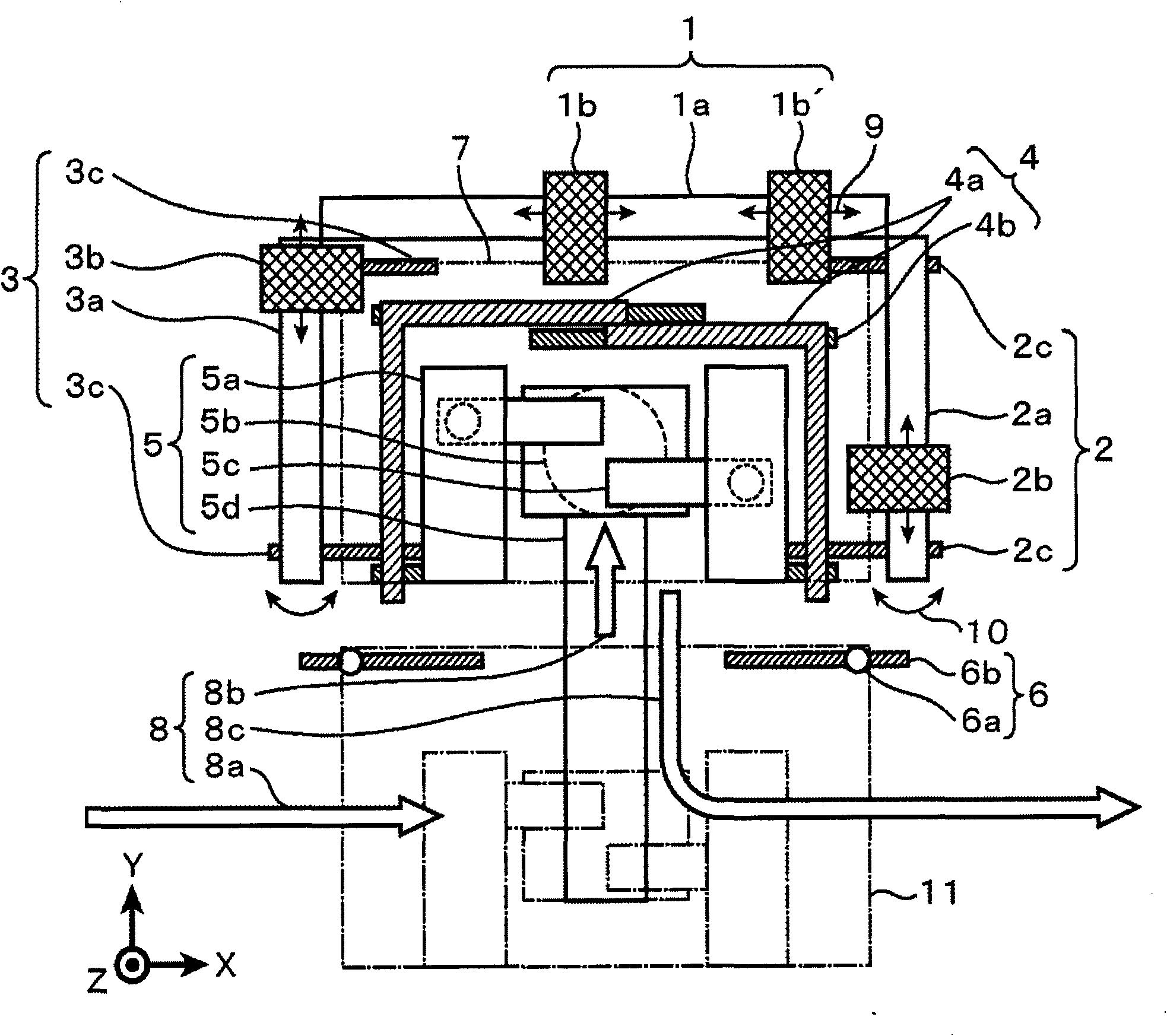
[0219] Figure 14 This is an example for explaining the configuration of a panel mounting apparatus and a panel conveying path for mounting panels using a conventional conveying method. The figure shows the state in which the whole panel assembly apparatus is viewed from obliquely above, and the panels are assembled while being transported between the units divided in the figure. Its flow is as follows.
[0220] (1) The process of cleaning the device mounting part of the edge part (electrode part) of the display panel
[0221] (2) The process of pasting an anisotropic conductive film (ACF: Anisotropic Conductive Film) on the edge of the display panel after cleaning
[0222] (3) The process of positioning and mounting the TAB and IC with high precision at the position where the ACF is pasted
[0223] (4) The process of thermocompression bonding the mounted TAB and IC and bonding them with the previous ACF film
[0224] (5) The pr...
Embodiment 3
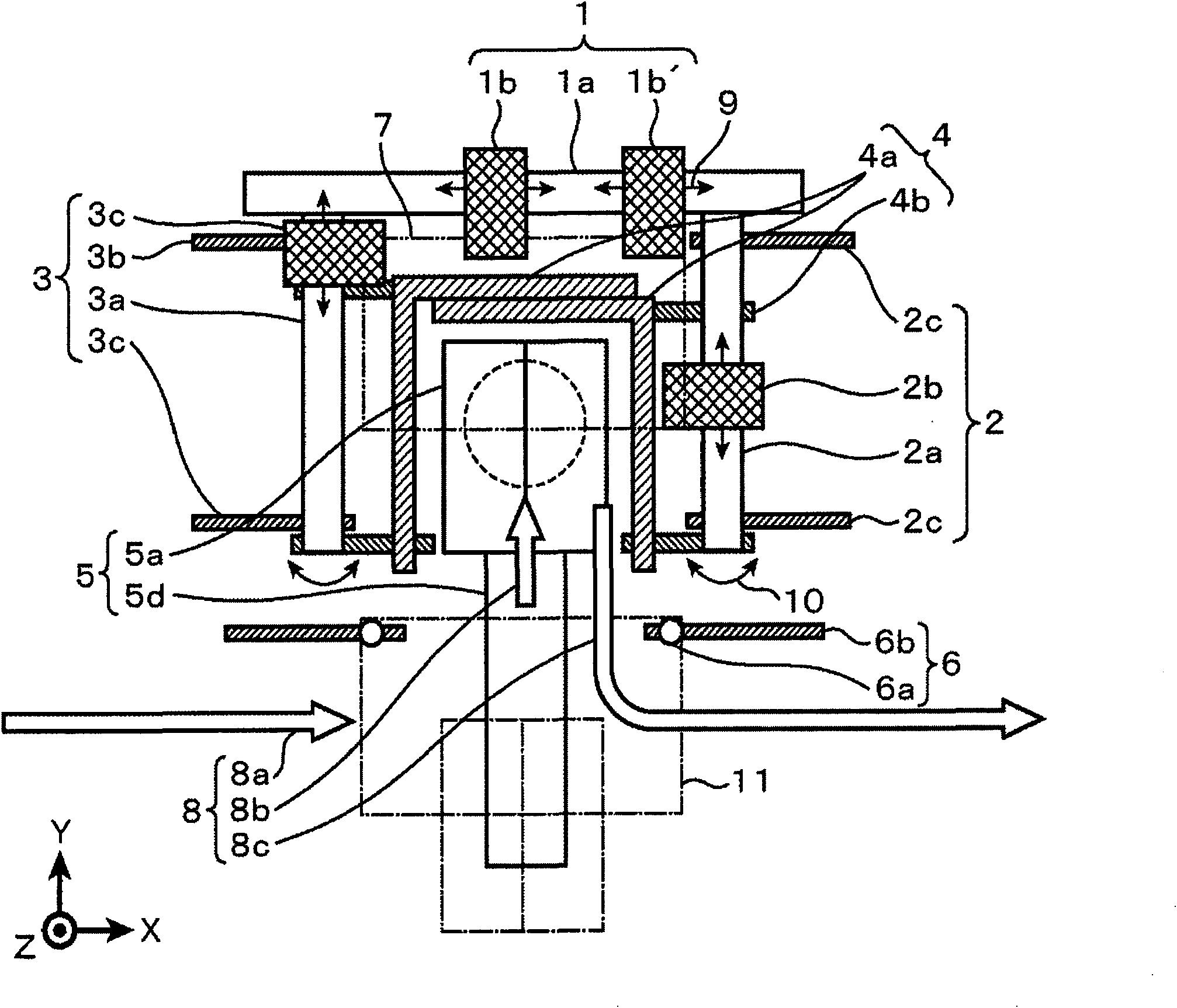
[0243] exist Figure 16 as well as Figure 17 In the plan view of , when the panel is carried into the panel edge processing unit 600 arranged in a "U" shape, the panel that has completed the edge processing remains in the panel edge processing unit 600; or when the panel that has completed the edge processing is carried out , When there is a display panel to be imported from the upstream, sometimes it is necessary to solve the collision between the panels, or to set a standby time on the side where the new import is to be carried out. In this case, even if the length of the device is shortened, the reduction in assembly time cannot be achieved due to the feature that simultaneous processing of the above-mentioned three sides can be realized. In addition, there is a possibility that the panel may be damaged, resulting in problems such as low reliability. Therefore, next, as Embodiment 3, the above-described Figure 16 as well as Figure 17 The method of solving the problems...
PUM
 Abstract
Description
Claims
Application Information
 - R&D Engineer
- R&D Manager
- IP Professional
- Industry Leading Data Capabilities
- Powerful AI technology
- Patent DNA Extraction
Browse by: Latest US Patents, China's latest patents, Technical Efficacy Thesaurus, Application Domain, Technology Topic, Popular Technical Reports.
© 2024 PatSnap. All rights reserved.Legal|Privacy policy|Modern Slavery Act Transparency Statement|Sitemap|About US| Contact US: help@patsnap.com