Method for making mask, method for performing optical proximity correction on layout pattern

An optical proximity correction and mask technology, applied in the semiconductor field, can solve the problems of long time, decreased process efficiency, complex layout pattern, etc.

Active Publication Date: 2011-11-30
SEMICON MFG INT (SHANGHAI) CORP +1
View PDF6 Cites 12 Cited by
  • Summary
  • Abstract
  • Description
  • Claims
  • Application Information

AI Technical Summary

Problems solved by technology

If this problem is to be solved, the lengths of the first extension section and the second extension section should be 70nm respectively, so that the pattern width h at the superposition position is 70nm; in practical applications, the layout pattern is very complicated, and the division position of the layout pattern is based on In the actual situation, the length of the extension at each split position depends on the specific situation, so that the width of the graphics at the superimposed position is equal to the target width. Due to the complexity of the layout graphics, determining the length of the extension at each split position will make the Process efficiency is reduced and time-consuming, so it is not feasible
[0007] The Chinese patent application with the application number "200710037440.4" discloses a graphical method, and the Chinese patent application with the application number "200810040372.1" discloses an optical proximity correction method, but none of them solve the above-mentioned problems

Method used


Image

  • Method for making mask, method for performing optical proximity correction on layout pattern
  • Method for making mask, method for performing optical proximity correction on layout pattern
  • Method for making mask, method for performing optical proximity correction on layout pattern

Examples


Embodiment Construction

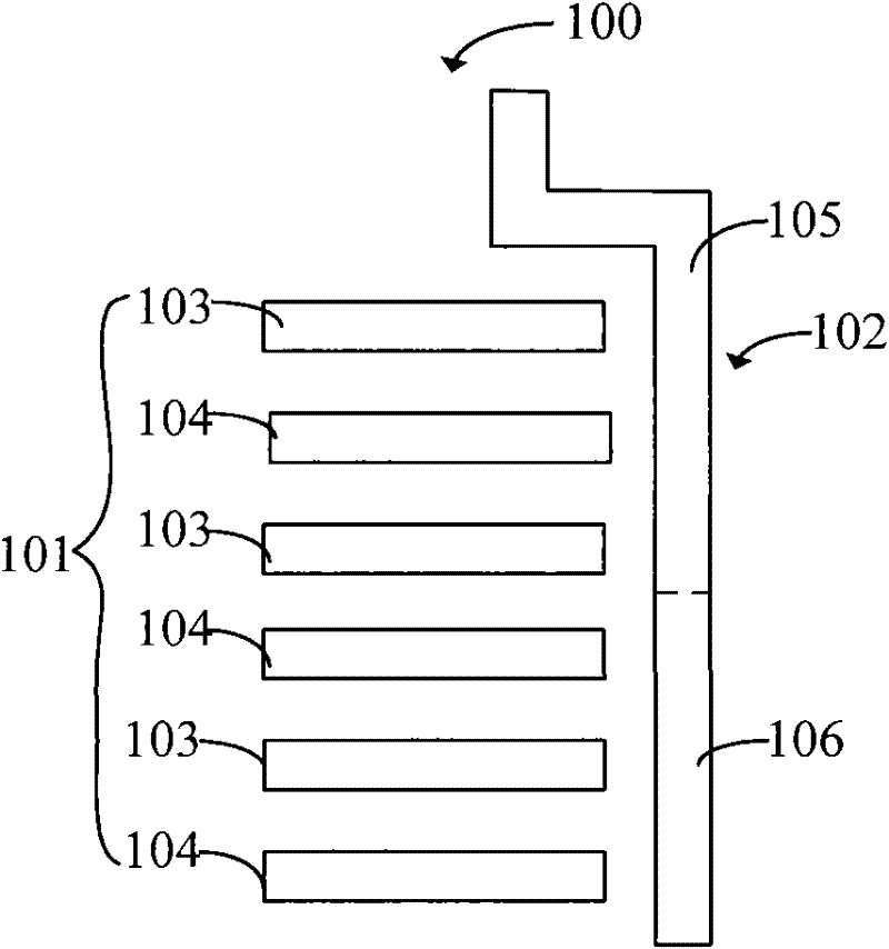
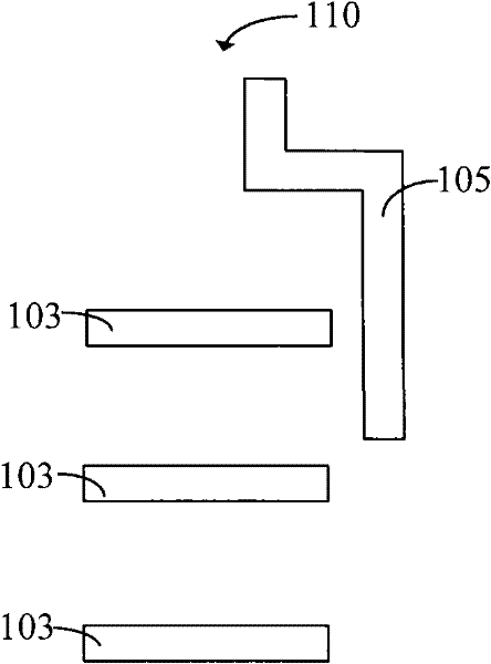
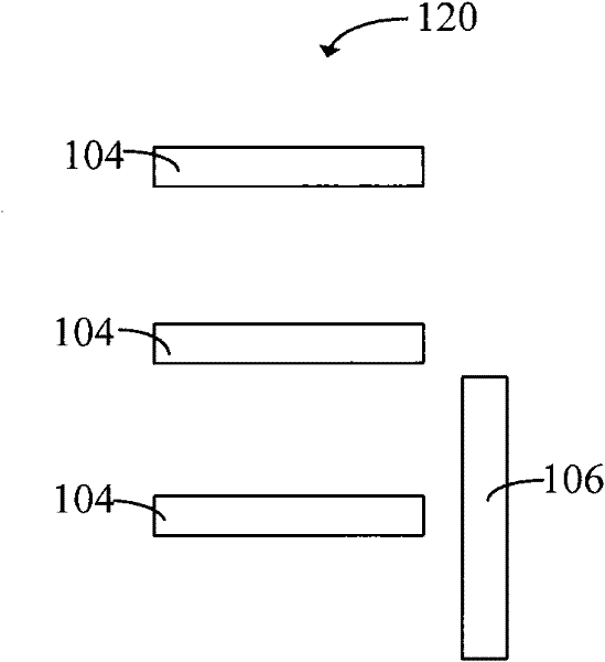
[0059] Specific embodiments of the present invention Perform optical proximity correction on the first layout graph and the first extension segment to obtain the first correction graph, which surrounds the area where the second extension segment is located after graphical simulation; execute the second Optical proximity correction of the layout pattern and the second extension section to obtain a second correction pattern, the second correction pattern encloses the area where the first extension section is located after graphical simulation; writing the first correction pattern into the first mask; Write the second modified pattern into the second mask; when patterning, when the first mask and the second mask are used as masks to form graphics, the width of the pattern is equal to the target width, at least the width of the pattern is the same as the target The gap between widths shrinks.

[0060] image 3 It is a flow chart of a method for forming a mask in a specific embodi...


PUM


Abstract

The invention relates to a method for producing masks, and an optical proximity correction method for layout patterns. The mask production method comprises steps that: a layout pattern is provided; the layout pattern is segmented into a first layout pattern and a second layout pattern; a first extension segment is formed at a segmentation position of the first layout pattern; a second extension segment is formed at a segmentation position of the second layout pattern; optical proximity correction is carried out upon the first layout pattern and the first extension segment such that a first corrected pattern is obtained, an area of the second extension segment is encircled by the first corrected pattern after graphic simulation; optical proximity correction is carried out upon the second layout pattern and the second extension segment such that a second corrected pattern is obtained, an area of the first extension segment is encircled by the second corrected pattern after graphic simulation; the first corrected pattern is wrote into a first mask; and the second corrected pattern is wrote into a second mask. During graphicalization, at an overlaying position, a pattern width is equal to a target width, and at least a difference between the pattern width and the target pattern width is reduced.

Description

technical field [0001] The invention relates to the technical field of semiconductors, in particular to a method for making a mask and an optical proximity correction method. Background technique [0002] The patterning process is a common process in the manufacture of semiconductor devices. It uses the mask as a mask to form the layout pattern on the photoresist layer on the semiconductor substrate to produce a photoresist layer printed on the photoresist layer. Resist layer pattern. [0003] As the critical dimensions of semiconductor devices become smaller and smaller, when the process node (half pitch) of the semiconductor process is less than 32nm, a mask is used as a mask under 193nm (nanometer) water immersion lithography conditions The patterning process of film formation has encountered physical limitations. The distance between adjacent patterns is too small. Due to the optical proximity effect, adjacent patterns will stick together. The solution in the prior art...

Claims


Application Information

Patent Timeline
Patent Type & Authority Applications(China)
IPC IPC(8): G03F1/14
Inventor 杨青
Owner SEMICON MFG INT (SHANGHAI) CORP
Why Eureka
Try Eureka