


Quick Research
Generate reliable direction feasibility study reports for your R&D in just a few steps.

Technical Q&A
Discover and master advanced knowledge NOW. Basics, ideas, possibilities, all at once.

Find Solutions
As an expert in R&D theories, this can generate solutions to your technical problems instantly.

Evaluate Feasibility
Analyze your overall solution with one click, know your potential R&D risks in advance.

Monitor Landscape
Get weekly tech updates, stay abreast of the latest tech innovations and key insights.
Three-dimensional semiconductor storing device and formation method thereof
A storage device and semiconductor technology, applied in semiconductor devices, semiconductor/solid-state device manufacturing, semiconductor/solid-state device components, etc., can solve problems such as product reliability reduction and process instability
- Summary
- Abstract
- Description
- Claims
- Application Information
AI Technical Summary
Problems solved by technology
Method used
Image

Examples
no. 1 example
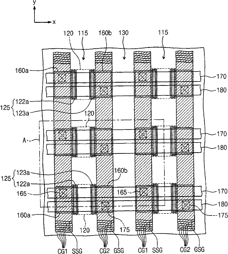
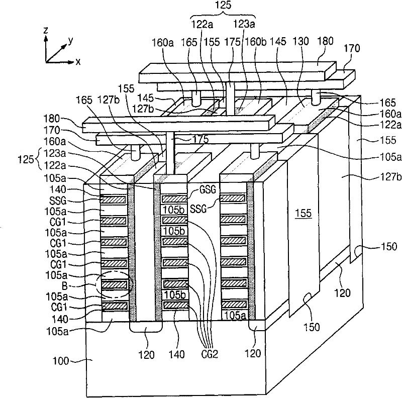
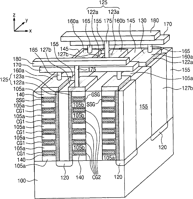
[0030] figure 1 is a plan view of a three-dimensional semiconductor memory device according to an embodiment of the inventive concept. Figure 2A is showing figure 1 A perspective view of part A. image 3 is showing Figure 2A Magnified view of part B. The three-dimensional semiconductor memory device may be a nonvolatile memory device.
[0031] refer to figure 1 and 2A , the first gate stack and the second gate stack may be disposed on a semiconductor substrate (hereinafter referred to as substrate) 100 laterally spaced apart from each other. The substrate 100 may be a silicon substrate, a germanium substrate or a silicon-germanium substrate. The substrate 100 may be doped with a first type dopant. For example, a well region doped with a first type dopant may be formed in the substrate 100 .
[0032] The first gate stack may include a first dielectric pattern 105a and first gates CG1 and SSG, the first dielectric pattern 105a and the first gates are alternately and r...
no. 2 example
[0109] Figure 8is a plan view illustrating a three-dimensional semiconductor memory device according to another embodiment of the inventive concept. Figure 9A is showing Figure 8 Perspective view of part C.
[0110] refer to Figure 8 and Figure 9A , the first gate stack and the second gate stack on the substrate 200 may extend side by side along the first direction. The substrate 200 may be a silicon substrate, a germanium substrate or a silicon germanium substrate. The substrate 200 may be doped with a first type dopant. The first gate stack may include alternately and repeatedly stacked first dielectric patterns 205a and first gates CGa1 and SSGa, and the second gate stack may include alternately and repeatedly stacked first gates CGa1 and SSGa on the substrate 200. The second dielectric pattern 205b on one side of the stack and the second gates CGa2 and GSGa.
[0111] The first gates CGa1 and SSGa included in the first gate stack may include a stacked plurality ...
PUM
 Abstract
Description
Claims
Application Information
 - R&D Engineer
- R&D Manager
- IP Professional
- Industry Leading Data Capabilities
- Powerful AI technology
- Patent DNA Extraction
Browse by: Latest US Patents, China's latest patents, Technical Efficacy Thesaurus, Application Domain, Technology Topic, Popular Technical Reports.
© 2024 PatSnap. All rights reserved.Legal|Privacy policy|Modern Slavery Act Transparency Statement|Sitemap|About US| Contact US: help@patsnap.com