
Light receiving-transmitting integral device

An optical transceiver and integrated technology, which is applied in the coupling of electric solid-state devices, semiconductor devices, and optical waveguides, can solve problems such as low integration and complex assembly structures, and achieve higher integration, lower costs, and simplified assembly processes and assemblies. structure effect

Inactive Publication Date: 2011-08-17
HUAWEI TECH CO LTD
View PDF3 Cites 14 Cited by
  • Summary
  • Abstract
  • Description
  • Claims
  • Application Information

AI Technical Summary

Problems solved by technology

[0006] An embodiment of the present invention provides an integrated optical transceiver device to overcome the defects of low integration and complex assembly structure of the optical transceiver integrated device in the prior art

Method used


Image

  • Light receiving-transmitting integral device
  • Light receiving-transmitting integral device
  • Light receiving-transmitting integral device

Examples


Embodiment Construction

[0017] In order to make the purpose, technical solutions and advantages of the embodiments of the present invention clearer, the technical solutions in the embodiments of the present invention will be clearly and completely described below in conjunction with the drawings in the embodiments of the present invention. Obviously, the described embodiments It is a part of embodiments of the present invention, but not all embodiments. Based on the embodiments of the present invention, all other embodiments obtained by persons of ordinary skill in the art without creative efforts fall within the protection scope of the present invention.

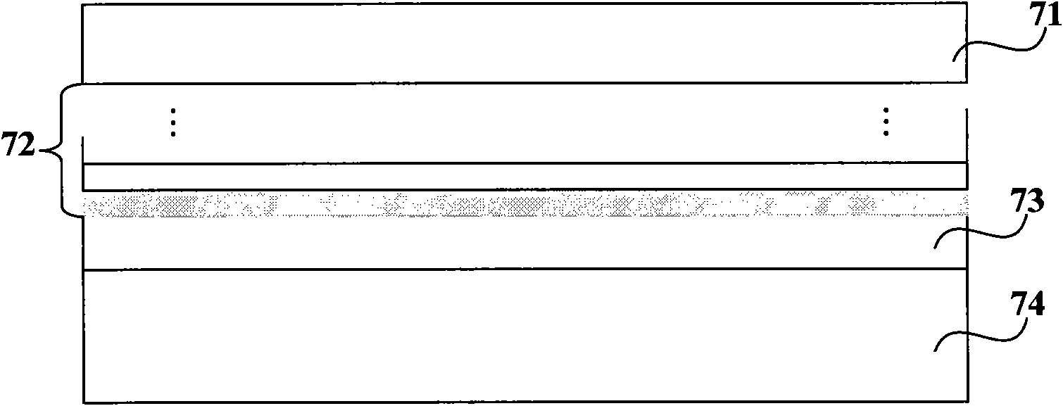
[0018] The optical transceiver integrated device provided by the embodiment of the present invention includes: a silicon (Si) substrate, an insulating layer of a semiconductor, and a Si layer attached to the insulating layer of the semiconductor; wherein, the insulating layer of the semiconductor can be silicon dioxide (SiO 2 ), may also include d...


PUM


Abstract

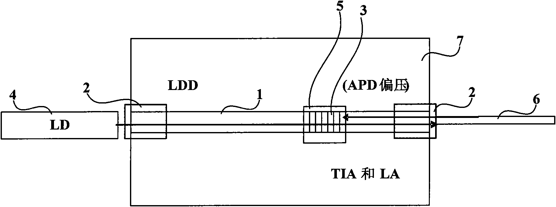
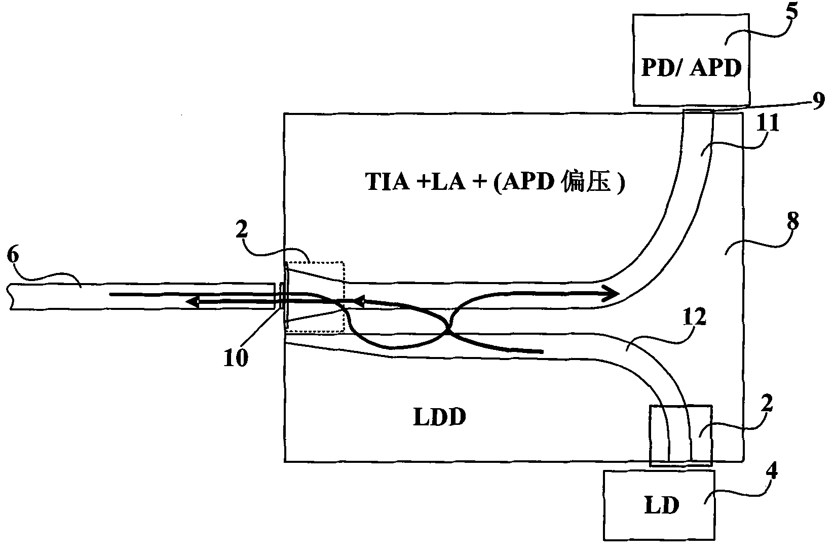
The invention discloses a light receiving-transmitting integral device, which comprises a silicon substrate, a semi-conductor insulating layer and a silicon layer adhered to the semi-conductor insulating layer, wherein the semi-conductor insulating layer is arranged between the silicon substrate and the silicon layer; the silicon layer is integrated with a laser driver, a trans-impedance amplifier, an amplitude-limiting amplifier, a waveguide and a spot-size converter; and a laser, a light detector or an avalanche photodiode are adhered to the surface of the silicon layer. By integrating the circuits required by the light receiving-transmitting integral device such as LDD (laser detector diode), TIA (totally integrated automation), LA (limiting amplifier), and the like, on the SOI (silicon on insulator) substrate, the size of the light receiving-transmitting integral device is reduced. Discrete light components such as LD (laser diode), PD (potential difference) / APD (avalanche photo diode) are adhered and assembled, thereby realizing the mixing integration of the light receiving-transmitting integral device, simplifying the assembling process, and effectively lowering the cost of the light receiving-transmitting integral device.

Description

technical field [0001] Embodiments of the present invention relate to an optical access terminal, and in particular to an integrated optical transceiver device. Background technique [0002] "Optical into copper out" has become the development trend of broadband access, but the relatively high cost of optical access terminals limits the development of optical access. [0003] The optical access terminal includes an optical transceiver module, that is, an optical module, also called an integrated optical transceiver device. Optical transceiver integrated device includes laser (Laser Diode, LD), photodetector (PhotodiodeDetector, PD) / avalanche photodiode (Avalanche Photodiodes, APD), mode spot converter (Spot-Size Converter, SSC), wavelength division multiplexing ( Wave Division Multiplexing (WDM) filter, Laser Diode Driver (LDD), Transimpedance amplifier (Transimpedance amplifier, TIA), Limiting Amplifier (Limiting Amplifier, LA) and / or APD bias circuit, waveguide, etc. A...

Claims


Application Information

Patent Timeline
Patent Type & Authority Applications(China)
IPC IPC(8): G02B6/42H01L27/00H01L27/12
Inventor 颜学进钟德刚易永江付生猛李胜平高建河
Owner HUAWEI TECH CO LTD
Learn More