Methods for manufacturing superjunction structure and superjunction semiconductor device
A technology of super-junction semiconductors and manufacturing methods, which is applied in semiconductor/solid-state device manufacturing, electrical components, circuits, etc., and can solve the difficulties of accurately controlling the height of silicon dioxide in the expanded trench, increasing process complexity, and small process tolerances, etc. problem, to achieve superior performance, easy filling and planarization, and increased process tolerance
- Summary
- Abstract
- Description
- Claims
- Application Information
AI Technical Summary
Problems solved by technology
Method used
Image
Examples
Embodiment 1
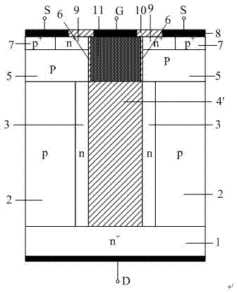
[0062] As a preferred embodiment of the present invention, the present invention discloses a novel superjunction semiconductor device structure (such as Figure 4h Shown) the manufacturing method, it comprises the steps:
[0063] a. By epitaxial growth, a p-type semiconductor drift region 2 of the first conductivity type is formed on the semiconductor substrate 1, such as Figure 4a shown;
[0064] b. On the semiconductor drift region 2 of the first conductivity type, etch toward the semiconductor substrate along the top of the semiconductor drift region of the first conductivity type until the semiconductor substrate 1, forming a first trench ;Such as Figure 4b shown. Dry etching such as reactive ion etching may be used, or wet etching may be used. The aspect ratio of the trench can be accurately controlled by dry etching, and the formed trench is basically U-shaped; the trench formed by wet etching can be trapezoidal or V-shaped. Preferably, dry etching is selected to ...
Embodiment 2
[0078] The manufacturing process of the semiconductor device of the present invention described in Embodiment 1 is preferably applied to a MOS control vertical device, so as to alleviate the contradictory relationship among withstand voltage, on-resistance and switching loss. Applied in such as Figure 5a when the IGBT device shown. The difference from Example 1 is that the initial semiconductor material substrate 1 is P + The semiconductor substrate 101 has the same conductivity type as the drift region of the first conductivity type. Its key steps are as Figure 5b shown. All the other steps are identical to Example 1.
Embodiment 3
[0080] The manufacturing process of the semiconductor device of the present invention described in Embodiment 1 can be applied to control vertical devices of N-channel MOS, and can also be applied to control vertical devices of P-channel MOS. P-channel VDMOS as Figure 6a shown. When used in the manufacture of P-channel MOS control vertical devices, the semiconductor substrate 1, the semiconductor layer 2 of the first conductivity type, the semiconductor drift region 3 of the second conductivity type formed by implantation at a small inclination angle, the active region 5, and the body contact region 7. The doping type of the source region 9 is opposite to that of the corresponding region of the N-channel MOS control vertical device. The key steps are as follows Figure 6b shown. In Embodiment 1, an N-channel VDMOS is manufactured, and N-type impurities are implanted at a small angle to form a semiconductor drift region 3 of the second conductivity type; A semiconductor dri...
PUM
 Abstract
Description
Claims
Application Information
 - R&D
- Intellectual Property
- Life Sciences
- Materials
- Tech Scout
- Unparalleled Data Quality
- Higher Quality Content
- 60% Fewer Hallucinations
Browse by: Latest US Patents, China's latest patents, Technical Efficacy Thesaurus, Application Domain, Technology Topic, Popular Technical Reports.
© 2025 PatSnap. All rights reserved.Legal|Privacy policy|Modern Slavery Act Transparency Statement|Sitemap|About US| Contact US: help@patsnap.com


