Anti-single event transient circuit

A transient circuit, anti-single event technology, applied in the direction of logic circuit connection/interface layout, logic circuit coupling/interface using field effect transistors, etc., can solve the problems of high area and power consumption, redundancy of latch units, etc. , to achieve the effect of simplified design, low power consumption and convenient implementation

Active Publication Date: 2012-08-22
BEIJING MXTRONICS CORP +1
View PDF4 Cites 0 Cited by
  • Summary
  • Abstract
  • Description
  • Claims
  • Application Information

AI Technical Summary

Problems solved by technology

Three-mode redundancy plus majority voting can basically eliminate the effect of single-event transients, but it will bring extremely high overhead (>200%) in area and power consumption
Time redundancy is lower in area and power consumption than triple-mode redundancy, but there are still three or more latch unit redundancy and additional speed overhead

Method used


Image

  • Anti-single event transient circuit
  • Anti-single event transient circuit
  • Anti-single event transient circuit

Examples


Embodiment Construction

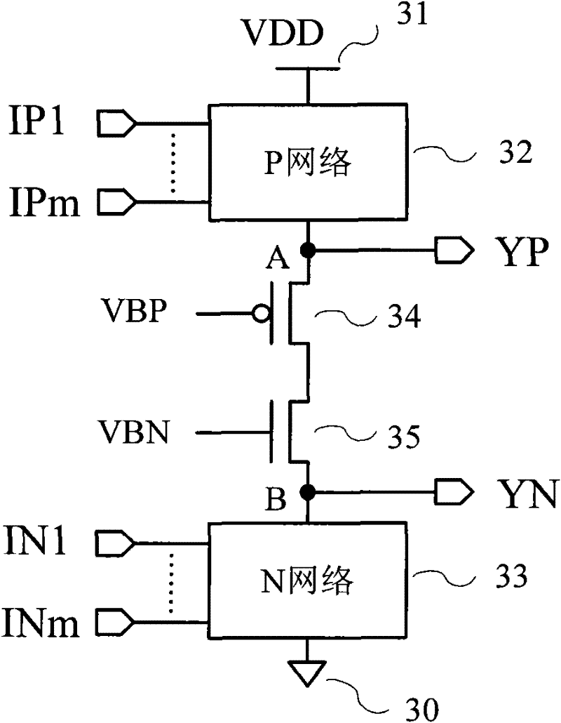
[0022] Such as image 3 Shown is the single-stage structure of the circuit of the present invention. The circuit is composed of power supply 31 (VDD), ground 30, P network 32, N network 33, and PMOS transistor 34 and NMOS transistor 35 between P network 32 and N network 33. P network 32 is connected to power supply 31 and PMOS transistor respectively. The source terminals of 34 are connected, and the output signal at the junction A of the P network 32 and the PMOS transistor 34 is YP, and the N network 33 is connected with the source terminals of the ground 30 and the NMOS transistor 35 respectively, and the N network 33 is connected with the NMOS transistor 35. The output signal at the connected node B is YN. The P network 32 is composed of PMOS transistor logic, that is, it is composed of several PMOS transistors connected in series and parallel. There may be multiple connection methods according to different functions. The N network 33 is composed of NMOS transistors. Logi...


PUM


Abstract

The invention discloses an anti-single event transient circuit, which is realized in a way that: the input of a P network and an N network of a complementary metal oxide semiconductor (CMOS) logic gate is separated to form P input and N input which are the redundancy of each other; a pair of series-wound P-channel metal oxide semiconductor (PMOS) transistor and N-channel metal oxide semiconductor(NMOS) transistor is inserted between the P network and the N network; and constant bias voltages are applied to the gate ends of the inserted pair of PMOS transistor and NMOS transistor to form two output nodes P output and N output which are the redundancy of each other. The circuit provided by the invention has the advantages of anti-single event transient capacity, simple structure, low powerconsumption and the like, and is applied to a digital logic circuit, a sequential circuit and a memory circuit.

Description

technical field [0001] The present invention relates to a circuit, and more particularly to a circuit capable of resisting single-event transients. Background technique [0002] The radiation produced by high-energy protons or high-energy neutrons hitting the atomic nucleus and the heavy nuclear particles in cosmic rays can cause changes in the state of the circuit, such as transients in combinational logic and bit flips in memory-like units. This effect is the effect of a single particle The result is often called single event effect. Single event effects can be divided into single event upset (SEU), recoverable single event latch (SEL), single event transient (SET) and other single event soft errors, and also include single event burn (SEB), single event Hard errors such as particle gate breakdown (SEGR), unrecoverable single event latch-up (SEL), etc. [0003] figure 1 Shown is a traditional complementary CMOS logic gate structure, which is composed of P network 12, N ...

Claims


Application Information

Patent Timeline
Patent Type & Authority Patents(China)
IPC IPC(8): H03K19/0185
Inventor 王亮岳素格赵元富
Owner BEIJING MXTRONICS CORP
Why Eureka
Try Eureka