Solar battery and manufacturing method thereof
A technology for a solar cell and a manufacturing method, applied in the field of solar cells, can solve the problems of decreased light transmittance of the back electrode, affecting the reflectivity of the reflective layer, and complicated process methods, so as to improve the overall efficiency performance, improve the reflectivity, and reduce the equipment. effect on material cost
- Summary
- Abstract
- Description
- Claims
- Application Information
AI Technical Summary
Problems solved by technology
Method used
Image
Examples
experiment example 1
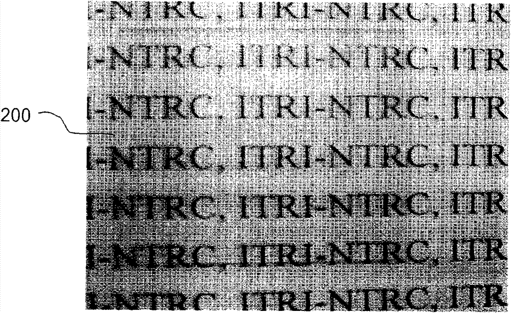
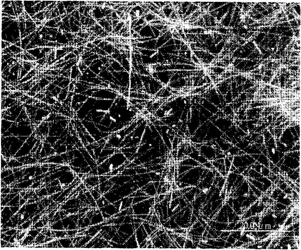
[0072] Figure 2A It is a transparent conductive film prepared according to Experimental Example 1. Figure 2B It is an image under an optical microscope of the transparent conductive film prepared according to Experimental Example 1.
[0073] In Experimental Example 1, a 0.2wt% nano-silver organic solution was used to evenly coat the glass substrate, and then the liquid was dried at a low temperature of about 50°C, thereby producing a transparent nano-silver conductive film with a thickness of about 0.5 μm. like Figure 2A As shown, the glass substrate 200 formed with the nano-silver conductive film of Experimental Example 1 is placed on the pattern, and it can be observed that the pattern under the glass substrate 200 can be clearly recognized even through the nano-silver conductive film. The fabricated nano-silver conductive film has high penetration. like Figure 2B As shown, the transparent nano-silver conductive film is observed under an optical microscope. The nano...
experiment example 2
[0079] Figure 3A It is a transparent conductive film prepared according to Experimental Example 2. Figure 3B It is an image under an optical microscope of the transparent conductive film prepared according to Experimental Example 2. Figure 3C It is a graph of the relationship between the transmittance of the transparent conductive film produced according to Experimental Example 2 and the wavelength of light. Figure 3D It is the I-V curve diagram of the transparent conductive film produced in the measurement experiment example 2.
[0080] In Experimental Example 2, 0.8wt% nano-silver organic solution was uniformly coated on the glass substrate, and a transparent nano-silver conductive film was fabricated in a manner similar to that of Experimental Example 1 above, with a thickness of about 0.8 μm. Next, carry out relevant tests as described in Experimental Example 1 to the nano-silver conductive film produced in Experimental Example 2, and the results are shown in Figur...
PUM
 Abstract
Description
Claims
Application Information
 - R&D
- Intellectual Property
- Life Sciences
- Materials
- Tech Scout
- Unparalleled Data Quality
- Higher Quality Content
- 60% Fewer Hallucinations
Browse by: Latest US Patents, China's latest patents, Technical Efficacy Thesaurus, Application Domain, Technology Topic, Popular Technical Reports.
© 2025 PatSnap. All rights reserved.Legal|Privacy policy|Modern Slavery Act Transparency Statement|Sitemap|About US| Contact US: help@patsnap.com


