Vanadium dioxide thin film phase transition characteristic-based terahertz wave modulation device and method
A technology of vanadium dioxide and phase change characteristics, applied in the field of terahertz wave application, can solve the problems of low switching efficiency and speed, and achieve the effect of fast phase change, high efficiency and fast speed
- Summary
- Abstract
- Description
- Claims
- Application Information
AI Technical Summary
Problems solved by technology
Method used
Image
Examples
Embodiment 1
[0019] The object of the present invention is achieved by the following technical solutions: a terahertz wave modulation device and method based on the phase change characteristics of a vanadium dioxide thin film. The modulation device is composed of a three-layer structure of a substrate, a vanadium dioxide thin film and a surface metal metamaterial. Among them, the vanadium dioxide film is uniformly grown on the surface of a silicon substrate with a thickness of 0.8 mm by a sol-gel method, and the film thickness is controlled at about 80 nm, and then the vanadium dioxide film is etched on the surface to prepare a metal metamaterial structure.
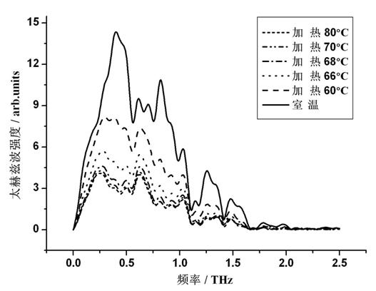
[0020] The vanadium dioxide film is excited by external heating to cause a reversible phase transition (SMT) between the monoclinic structure semiconductor phase vanadium dioxide (M) and the tetragonal structure metal phase vanadium dioxide (R). When the temperature rises above 68℃, the vanadium dioxide film changes from semiconductor ph...
Embodiment 2
[0022] The object of the present invention is achieved by the following technical solutions: a terahertz wave modulation device and method based on the phase change characteristics of a vanadium dioxide thin film. The modulation device is composed of a three-layer structure of a substrate, a vanadium dioxide thin film and a surface metal metamaterial. Among them, the vanadium dioxide film is uniformly grown on the surface of a quartz substrate with a thickness of 1 mm by a magnetron sputtering method, and the film thickness is controlled at about 600 nm, and then the vanadium dioxide film is etched on the surface to prepare a metal metamaterial structure.
[0023] An external laser with a wavelength of 600nm and a power of 400mW is used to excite the vanadium dioxide film to cause a reversible phase transition (SMT) between the monoclinic structure semiconductor phase vanadium dioxide (M) and the tetragonal structure metal phase vanadium dioxide (R) ). In the process of transiti...
Embodiment 3
[0025] The object of the present invention is achieved by the following technical solutions: a terahertz wave modulation device and method based on the phase change characteristics of a vanadium dioxide thin film. The modulation device is composed of a three-layer structure of a substrate, a vanadium dioxide thin film and a surface metal metamaterial. Among them, the vanadium dioxide film is uniformly grown on the surface of a sapphire substrate with a thickness of 2 mm by vapor deposition, and the film thickness is controlled at about 200 nm, and then the vanadium dioxide film is etched on the surface to prepare a metal metamaterial structure.
[0026] First, use an external electric field to preset the film to 35°C, and then input a 20V DC voltage signal to make the vanadium dioxide film produce monoclinic structure semiconductor phase vanadium dioxide (M) and tetragonal structure metal phase vanadium dioxide (R ) Reversible phase transition (SMT). In the process of transition...
PUM
| Property | Measurement | Unit |
|---|---|---|
| Thickness | aaaaa | aaaaa |
| Thickness | aaaaa | aaaaa |
Abstract
Description
Claims
Application Information
 - R&D
- Intellectual Property
- Life Sciences
- Materials
- Tech Scout
- Unparalleled Data Quality
- Higher Quality Content
- 60% Fewer Hallucinations
Browse by: Latest US Patents, China's latest patents, Technical Efficacy Thesaurus, Application Domain, Technology Topic, Popular Technical Reports.
© 2025 PatSnap. All rights reserved.Legal|Privacy policy|Modern Slavery Act Transparency Statement|Sitemap|About US| Contact US: help@patsnap.com


