
Concave-surface image sensor

An image sensor, concave technology, applied in the field of image sensors, can solve the problems of dislocation, panoramic picture dislocation, large difference in top resolution, etc.

Inactive Publication Date: 2011-05-25
任永斌
View PDF4 Cites 6 Cited by
  • Summary
  • Abstract
  • Description
  • Claims
  • Application Information

AI Technical Summary

Problems solved by technology

The more pixels a CCD contains, the higher the picture resolution it provides. The CCD acts like a film, but it converts image pixels into digital signals. At present, CCD image sensors and CMOS image sensors The pixels are neatly arranged on a flat semiconductor, that is, each pixel is on the same plane, which makes the resolution of different parts of the photo taken slightly different, and the resolution of the middle part of the picture is slightly higher than that of the surrounding area. Higher, the higher the intermediate resolution, that is, the resolution of the image formed by the scene at a unit angle is different. If you browse a single picture, this difference is difficult to find with the naked eye, but when we edit multiple pictures into a panorama When taking pictures, this difference may be found, and the edited pictures will appear misaligned. Now many people like Google Earth. When you browse the street view of Google Earth, you will find that some panoramic pictures are misaligned, especially the resolution at the top. The rate is quite different from other parts, which greatly affects the image of the environment to be perfectly reproduced

Method used


Image

  • Concave-surface image sensor
  • Concave-surface image sensor

Examples


Embodiment Construction

[0009] In the embodiment of the accompanying drawings, we take the implementation of a concave image sensor as an example to further illustrate the present invention:

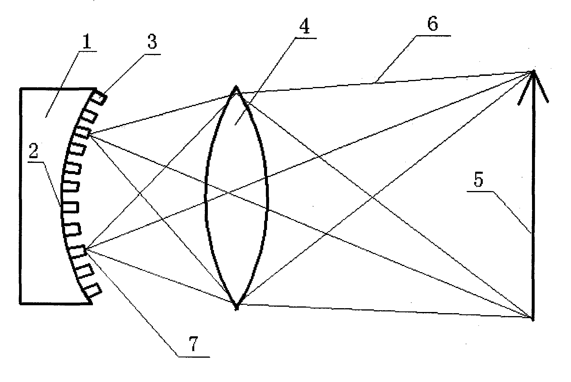
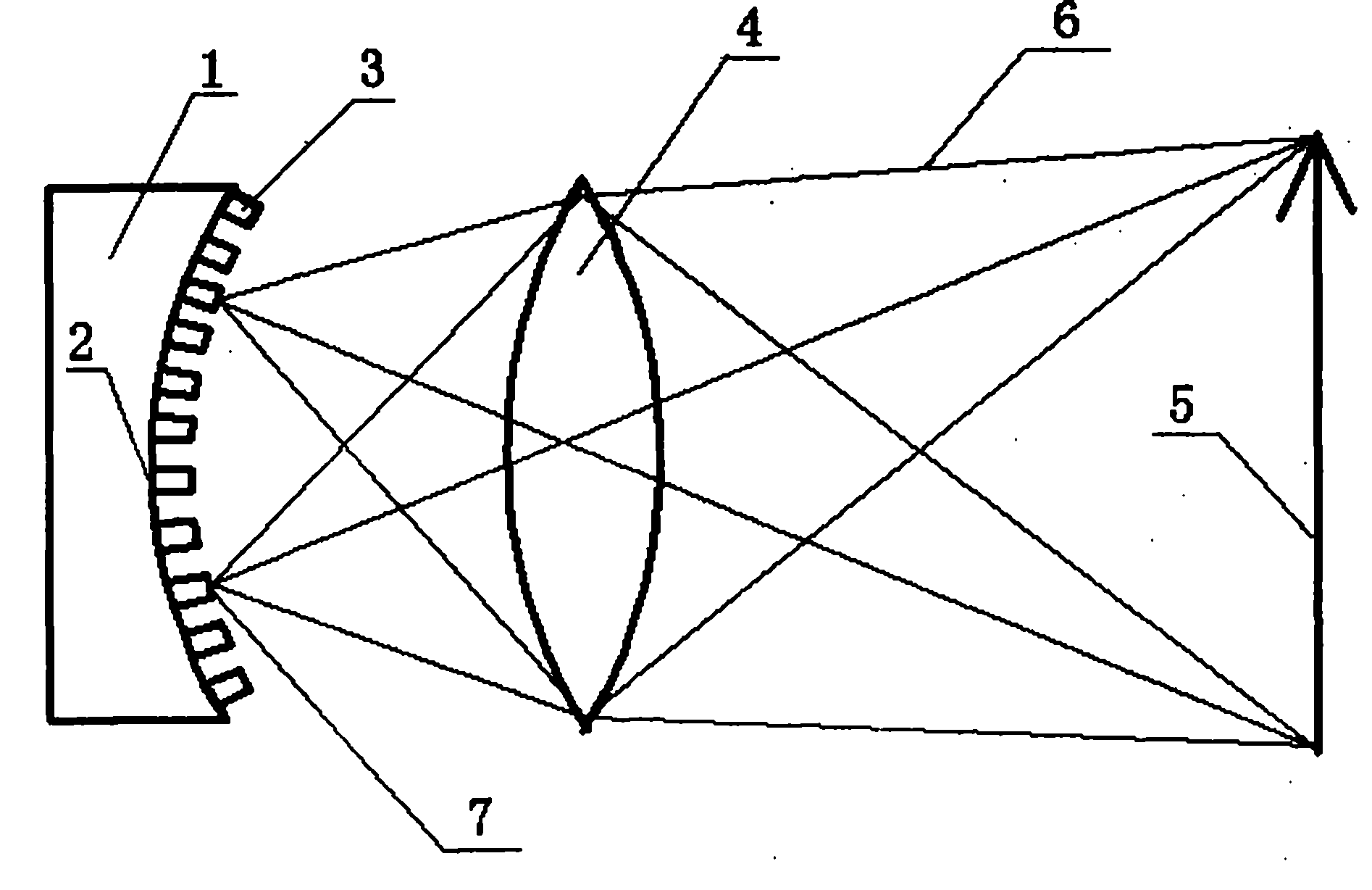
[0010] In the accompanying drawings, there is a semiconductor concave surface 2 on a semiconductor substrate 1, and pixels 3 are evenly distributed on the semiconductor concave surface 2, and the light reflected on the object 5 is focused on the intersection point between the object and the pixel by the convex lens 4 along the light path 6. 7, of course, the convex lens 4 can also be replaced by a pinhole. When the surface of the CCD is irradiated by light, each photosensitive unit, that is, the pixel 3, will reflect the charge on the component, and the signals generated by all photosensitive units are added together to form a For a complete picture, CCD can convert light into electric charge, and convert it into digital signal through analog-to-digital converter chip. After the digital signal is compressed, it ...


PUM


Abstract

The invention relates to a concave-surface image sensor, wherein a semiconductor concave surface is arranged on a semiconductor substrate, pixels are uniformly arranged on the semiconductor concave surface, and the ray reflected on a subject is imaged on the pixels through a convex lens or a pinhole. In the invention, the pixel arrangement of a traditional CCD (Charge-Coupled Device) image sensor and an MOS (Metal Oxide Semiconductor) image sensor is adjusted, and the pixels originally arranged on a plane are changed to be arranged on a concave surface, so that the resolutions of any parts at a unit angle of a shot scenery photo are all the same, the shot pictures are not dislocated when being spliced, the spliced panoramic picture is not dislocated when being seen from the front, rear, left, right, upper and lower directions, and the concave-surface image sensor is particularly suitable for being applied to street-scene views similar to Google Earth.

Description

Technical field [0001] The invention relates to an image sensor, especially a CCD or CMOS sensor in which the pixels (photosensitive units) of the photographs that can be seamlessly connected into a panoramic picture are distributed on a concave semiconductor substrate. Background technique [0002] CCD image sensors and CMOS image sensors are widely used in digital cameras and digital cameras. The main difference between CCD and CMOS in manufacturing is that CCD is integrated on a semiconductor single crystal material, while CMOS is integrated on a semiconductor called a metal oxide. In terms of materials, there is no essential difference in the working principle. For the sake of simplicity, the CCD image sensor is mainly mentioned below. CCD is a semiconductor device that can convert optical images into digital signals. The tiny photosensitive substances implanted on the CCD are called pixels. The more pixels a CCD contains, the higher the picture resolution it provides. ...

Claims


Application Information

Patent Timeline
Patent Type & Authority Applications(China)
IPC IPC(8): H01L27/146H04N5/335H04N5/369H04N25/00
CPCH04N25/702
Inventor 任永斌
Owner 任永斌
Learn More