


Quick Research
Generate reliable direction feasibility study reports for your R&D in just a few steps.

Technical Q&A
Discover and master advanced knowledge NOW. Basics, ideas, possibilities, all at once.

Find Solutions
As an expert in R&D theories, this can generate solutions to your technical problems instantly.

Evaluate Feasibility
Analyze your overall solution with one click, know your potential R&D risks in advance.

Monitor Landscape
Get weekly tech updates, stay abreast of the latest tech innovations and key insights.
Optical module and manufacturing method thereof
A manufacturing method and optical module technology, applied in semiconductor/solid-state device manufacturing, electrical components, electrical solid-state devices, etc., can solve problems such as chip function failure and packaging failure, achieve high-temperature aging without failure, reduce the probability of failure, and produce finished products rate-enhancing effect
- Summary
- Abstract
- Description
- Claims
- Application Information
AI Technical Summary
Problems solved by technology
Method used
Image


Examples
Embodiment Construction
[0013] In order to make the object, technical solution and advantages of the present invention clearer, the present invention will be described in further detail below in conjunction with specific embodiments and with reference to the accompanying drawings.
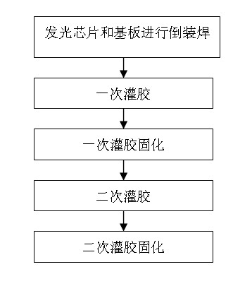
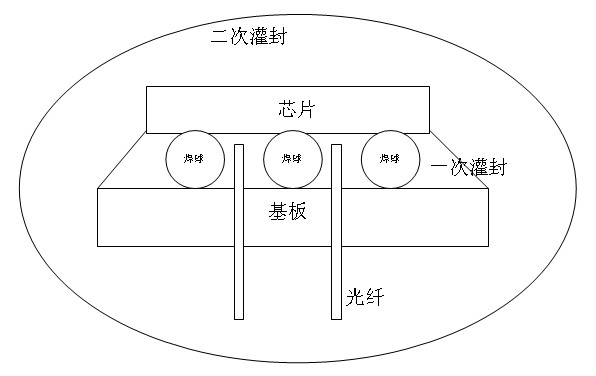
[0014] A package structure of an optical module disclosed in the present invention is attached figure 1 . The optical module includes a substrate and a chip that is flip-chip-bonded with the substrate. The space between the substrate and the chip is potted with transparent silicone, and the outside of the substrate and the chip is potted with potting glue.
[0015] In potting, EXF1000 glue dispenser can be used, and the thickness of the glue is about 20-25 microns. Transparent silica gel is used for the first potting, and its model is preferably OE6551 silica gel, and its CTE is 210±100ppm / °C. After dispensing, heat the optical module in an oven, preferably to 90±5°C, and continue heating for 240 minutes, then cool natu...
PUM
 Abstract
Description
Claims
Application Information
 - R&D Engineer
- R&D Manager
- IP Professional
- Industry Leading Data Capabilities
- Powerful AI technology
- Patent DNA Extraction
Browse by: Latest US Patents, China's latest patents, Technical Efficacy Thesaurus, Application Domain, Technology Topic, Popular Technical Reports.
© 2024 PatSnap. All rights reserved.Legal|Privacy policy|Modern Slavery Act Transparency Statement|Sitemap|About US| Contact US: help@patsnap.com