Detection method used for failure analysis of semiconductor device

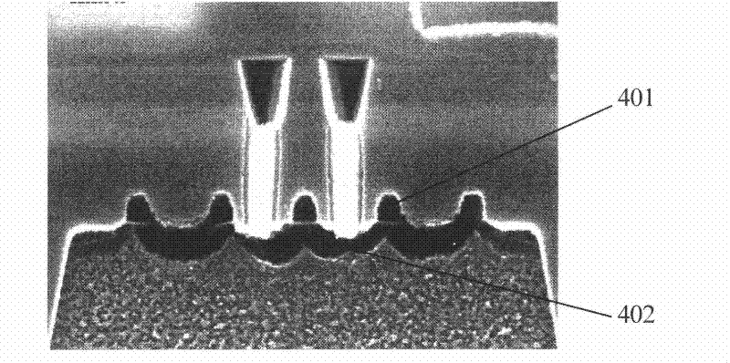
A detection method and failure analysis technology, which is applied in the direction of semiconductor/solid-state device testing/measurement, preparation of test samples, etc., and can solve the problem of poor observation effect, fast corrosion speed, semiconductor device gate region 401 or source/drain region 402 Destruction and other problems, to achieve high integrity, low corrosion damage, easy to observe and detect the effect

Active Publication Date: 2012-08-22
SEMICON MFG INT (SHANGHAI) CORP +1
View PDF3 Cites 0 Cited by
  • Summary
  • Abstract
  • Description
  • Claims
  • Application Information

AI Technical Summary

Problems solved by technology

However, due to the miniaturization of the size of semiconductors, especially for the 65nm process and below, the junction depth is shallow, and the problem of over-etching often occurs when using an etching solution.
figure 1 It is the secondary electron image picture after the semiconductor device is corroded by the corrosion treatment solution, such as figure 1 As shown, after being corroded by the etching treatment solution, the gate region 401 or the source / drain region 402 in the semiconductor device is damaged, which cannot truly reflect the depth of the source / drain region, resulting in poor observation effect and unable to accurately locate the position of the defect.
When the corrosion time is reduced to about 1 second to 2 seconds, the corrosion speed is too fast, the control is difficult, the repeatability and reliability of the corrosion treatment are poor

Method used


Image

  • Detection method used for failure analysis of semiconductor device
  • Detection method used for failure analysis of semiconductor device
  • Detection method used for failure analysis of semiconductor device

Examples


Embodiment Construction

[0029] It is known from the background art that the inventor of the present invention found that in the failure analysis of semiconductor devices, it is easy to cause over-corrosion to the semiconductor device and damage the semiconductor device when the corrosive corrosion treatment solution is usually used directly to corrode the semiconductor device to be analyzed. Moreover, this traditional chemical coloring treatment method cannot effectively highlight the junction and well levels of the semiconductor device, and cannot provide a basis for judging the failure of the source / drain junction of the device.

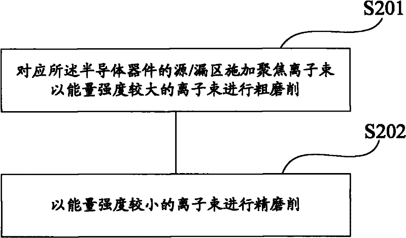
[0030] Therefore, in the manufacturing process of semiconductor devices, the inventor of the present invention envisages the use of focused ion beam grinding technology to first change the surface properties of the junction profile to make it in an over-stressed state, and then use an etching solution for subsequent etching to be able to Under the condition of not causing ove...


PUM


Abstract

The invention relates to a detection method used for failure analysis of a semiconductor device, comprising the following steps of: grinding a deficient section of the semiconductor device by utilizing a focused ion beam so as to change surface property of a source / drain region; corroding the section of the semiconductor device by utilizing a corrosion treatment solution so as to expose the section feature of the source / drain region; and obtaining image information corresponding to the section of the semiconductor device by utilizing an amplifying imaging device, and observing the image information to obtain the distribution condition of the defect generated by the semiconductor device. In the invention, through the combination of grinding of the focused ion beam and corroding of the corrosion treatment solution, the section feature of the source / drain region of the semiconductor device which is easily observed is obtained, and the basis of judging whether the device is in failure or not is provided.

Description

Technical field [0001] The present invention relates to the field of semiconductor manufacturing, in particular to a detection method for failure analysis of semiconductor devices. Background technique [0002] For the mass production of semiconductor devices, it is desirable to be able to provide profitable and reliable process technology. The process for improving the reliability and stability of the process technology includes the steps of designing a semiconductor device, manufacturing a sample of the semiconductor device, and testing the sample. Failure analysis of semiconductor devices is a feedback process that involves finding and correcting the root causes of defects to overcome the problems caused by the defects. [0003] Proper failure analysis is critical to improving the quality of semiconductor devices. Incorrect failure analysis may lengthen the cycle required to develop and upgrade semiconductor device products. Generally, failure analysis includes external inspe...

Claims


Application Information

Patent Timeline
Patent Type & Authority Patents(China)
IPC IPC(8): H01L21/66G01N1/32
Inventor 陈险峰韩耀梅苏凤莲任正鹏王玉科
Owner SEMICON MFG INT (SHANGHAI) CORP
Why Eureka
Try Eureka