
Pixel array

A pixel array and pixel technology, applied in the field of pixel array, can solve the problems of power consumption, pressure loss panel, insufficient resolution, etc., and achieve the effects of avoiding damage, high luminous efficiency and service life, and improving positioning resolution

Inactive Publication Date: 2011-04-20
AU OPTRONICS CORP
View PDF5 Cites 2 Cited by
  • Summary
  • Abstract
  • Description
  • Claims
  • Application Information

AI Technical Summary

Problems solved by technology

[0005] However, for the above-mentioned touch panel, its sensing method belongs to the "contact pressurization" sensing method, so there will be a problem of insufficient resolution, and when inputting to the touch panel, it is quite easy. The problem of pressure damage to the panel due to excessive contact force
[0006] Moreover, since the touch panel is attached to the outermost layer of the display panel, images must pass through the touch panel to be displayed, which will reduce the luminous efficiency of the panel, not only consume more power, but also shorten the lifespan of the display panel. service life

Method used


Image

  • Pixel array
  • Pixel array
  • Pixel array

Examples


Embodiment Construction

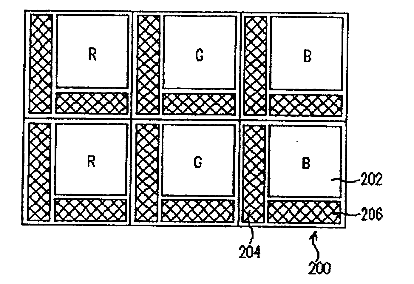
[0034] figure 2 What is shown is a schematic plan configuration diagram of a pixel array in a preferred embodiment of the present invention. Generally speaking, the pixel array on the display panel is composed of a plurality of pixels arranged in an array. For simplicity, in figure 2 Only some (6) pixel structures are shown in . Moreover, the pixel array of the present invention may be a pixel array for a liquid crystal display panel, or a pixel array for an organic electroluminescent display panel.

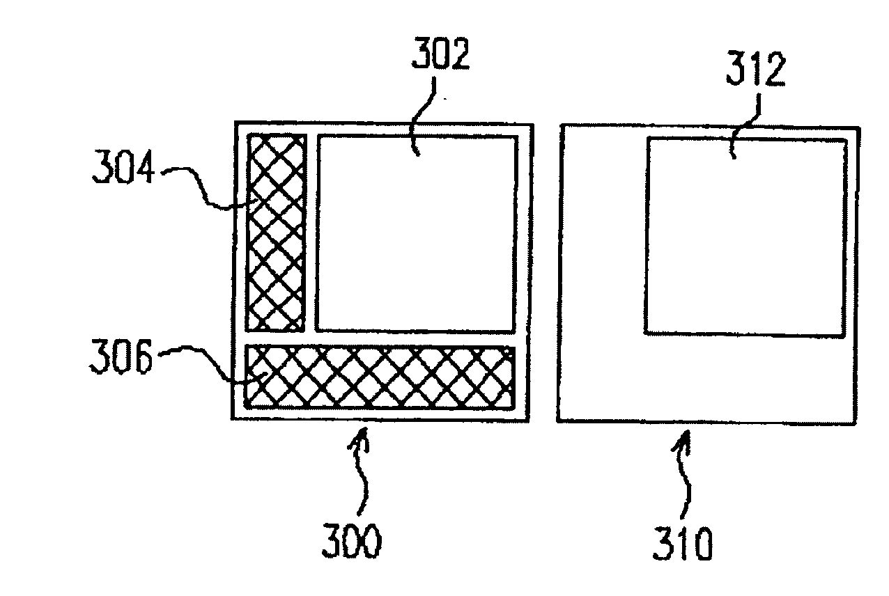
[0035] Please refer to figure 2 , each pixel structure 200 in the pixel array has at least one sub-pixel (sub-pixel) 202 and one addressable pixel (shadow pixel) 204 . Each sub-pixel 202 is, for example, one of a sub-pixel displaying red (R), a sub-pixel displaying green (G), or a sub-pixel displaying blue (B). The arrangement of the sub-pixels 202 is, for example, a mosaic type, a triangle type, a stripe type or a four-pixel RGGB configuration type (not shown).

[0036] ...


PUM


Abstract

A pixel array is composed of a plurality of pixel structures in array arrangement, and each pixel structure at least comprises a sub-pixel and an address pixel, wherein the addressing pixel is configured at one side of the sub-pixel and can generate electromagnetic radiation wave with invisible wavelength. The addressing pixel in the pixel array is properly arranged so that the pixel array can be divided into a plurality of groups of digital codes; therefore, the pixel array can be applied to constructing a non-touch panel input device by detecting a digital code combination composed of electromagnetic radiation wave generated by the addressing pixel.

Description

[0001] The patent application of the present invention is a divisional application of the patent application for invention with the application number 03130892.9 and the invention name "Pixel Array" filed by the applicant on May 21, 2003. technical field [0002] The present invention relates to a pixel array, and in particular to a pixel array in which addressable pixels are arranged in a pixel structure, which can be applied to construct a non-contact panel input device. Background technique [0003] With the rapid development and application of information technology, wireless mobile communication and information home appliances, many information products have changed from traditional input methods to touch panel (Touch Panel) is used as an input device, so the space occupied by input devices such as a keyboard or a mouse can be saved. [0004] Please refer to figure 1 , which represents a schematic cross-sectional view of a well-known touch panel, wherein the touch pane...

Claims


Application Information

Patent Timeline
Patent Type & Authority Applications(China)
IPC IPC(8): G06F3/041
Inventor 张浥塵胡硕修
Owner AU OPTRONICS CORP
Learn More