
Electrical model of accumulation type MOS varactor

A MOS tube and varactor technology, which is applied in the field of electrical models of accumulative MOS varactors, can solve the simulation accuracy that cannot reach the design accuracy of radio frequency integrated circuits, the electrical model is too simple, and the modulation characteristics of devices of different sizes are lacking. It can improve the efficiency and practicability, and the effect of good fitting ability.

Active Publication Date: 2011-03-30
SHANGHAI HUAHONG GRACE SEMICON MFG CORP
View PDF2 Cites 7 Cited by
  • Summary
  • Abstract
  • Description
  • Claims
  • Application Information

AI Technical Summary

Problems solved by technology

The current electrical model of the accumulation type MOS varactor is often too simple, lacks the ability to fit the modulation characteristics of devices of different sizes, and the simulation accuracy cannot meet the requirements of the design accuracy of radio frequency integrated circuits

Method used


Image

  • Electrical model of accumulation type MOS varactor
  • Electrical model of accumulation type MOS varactor
  • Electrical model of accumulation type MOS varactor

Examples


Embodiment Construction

[0023] The modeling method of the accumulation type MOS varactor in the present invention is divided into two steps.

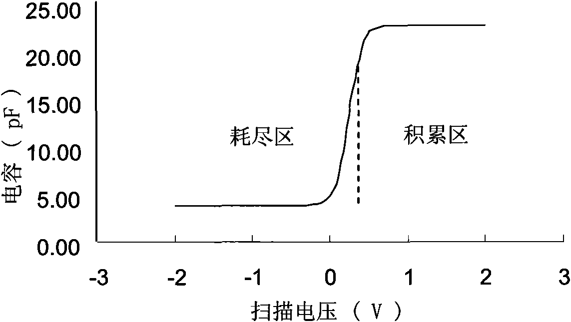
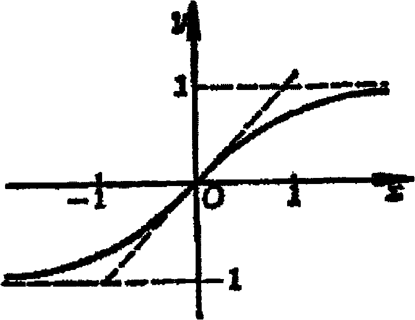
[0024] The first step is to select the basic functions. Comparing the modulation characteristic curve of the accumulation MOS varactor with the curve of the commonly used function in the field of mathematics, it is found that the curve of the hyperbolic tangent function is relatively similar to it.

[0025] see image 3 , which is the basic curve of the hyperbolic tangent function, The curve is between the horizontal straight lines y=1 and y=-1, and monotonously increases in any x range.

[0026] The second step is to modify and deform the basic functions. On the basis of the hyperbolic tangent function, considering the physical meaning of the accumulation type MOS varactor, one or more model parameters are determined.

[0027] After repeated tests and comparisons, the electrical model of the accumulated MOS varactor finally determined is:

[0028] ...


PUM


Abstract

The present invention discloses a method of matching accumulation type MOS varactor electrical properties, adopting capacitance Cap of formula computing accumulation type MOS varactor. Vgs is voltage applied between the grid electrode and source electrode of the accumulation type MOS varactor, and the grid electrode is taken as a variable voltage terminal, and the source electrode and a drain electrode are shorted, so as to form a reference voltage terminal; tanh() is a hyperbolic tangent function; c1=a+b*Wg+c*Lg+d*Wg*Lg, c2=e*Wg*Lg, wherein a, b, c, d and e are constant and range from 0 to 10; Wg and Lg are channel width and channel lengthof the accumulation type MOS varactor respectively; and c3 and c4 are constant and range from minus 2 to 2. The model has good fitting capability on various accumulation type MOS varactors with different channel lengths and different channel widths.

Description

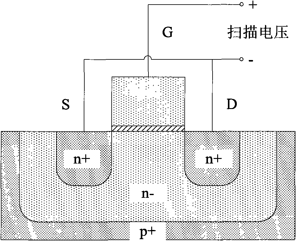
technical field [0001] The invention relates to a model method of a semiconductor device, in particular to a model of a MOS varactor. Background technique [0002] MOS varactor (MOS varactor) is one of the radio frequency devices commonly used in semiconductor radio frequency integrated circuits. Commonly used MOS varactors include inversion mode and accumulation mode. [0003] see figure 1 , which is a schematic diagram of an accumulation MOS varactor. Among them, G, S, and D represent the gate, source, and drain of the MOS varactor, respectively, and n+, n-, and p+ represent the n-type heavily doped region, n-type lightly doped region, and p-type heavily doped region, respectively. . The accumulation type MOS varactor is an np type MOS transistor, that is, on the basis of PMOS, the p-type heavily doped regions of the source and drain are replaced with n-type heavily doped regions. [0004] In actual work, the gate G of the accumulation MOS varactor is used as the varia...

Claims


Application Information

Patent Timeline
IPC IPC(8): G06F17/50
Inventor 周天舒
Owner SHANGHAI HUAHONG GRACE SEMICON MFG CORP
Learn More