
InP-based strained quantum well structure with pseudo-substrate and preparation method thereof

A quantum well and substrate technology, which is applied in the field of InP-based strained quantum well structure and preparation, can solve the problems of single-layer potential well or barrier layer thickness limitation, and achieve the effects of increasing critical thickness, good versatility, and improving quality

Inactive Publication Date: 2012-05-30
弦海(上海)量子科技有限公司
View PDF0 Cites 0 Cited by
  • Summary
  • Abstract
  • Description
  • Claims
  • Application Information

AI Technical Summary

Problems solved by technology

In order to obtain a longer luminous wavelength, it is necessary to control the total strain of the mismatched quantum well. Designing a strain compensation structure is a major way. The layer thickness of the well or barrier is still limited

Method used


Image

  • InP-based strained quantum well structure with pseudo-substrate and preparation method thereof
  • InP-based strained quantum well structure with pseudo-substrate and preparation method thereof
  • InP-based strained quantum well structure with pseudo-substrate and preparation method thereof

Examples


Embodiment 1

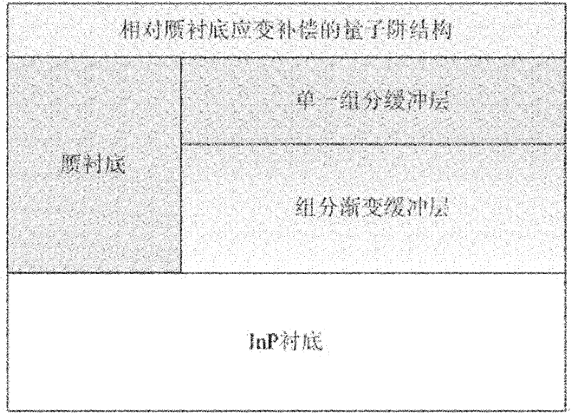
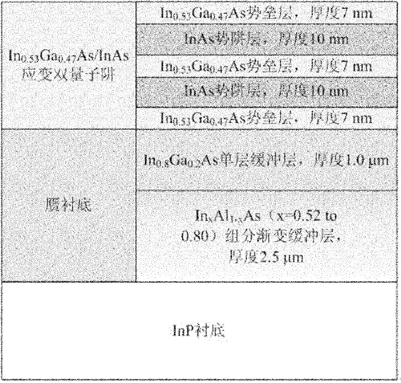
[0030] (1) Using molecular beam epitaxy to grow materials, such as figure 2 As shown, the thickness of the InAs potential well layer in the quantum well is 10nm, and the InAs 0.53 Ga 0.47 The thickness of the As barrier layer is 7nm, and the quantum well structure is relatively In 0.8 Ga 0.2 The As single-layer buffer layer constitutes strain compensation, and the number of quantum wells is taken as 2, that is, a double quantum well structure is grown. If the quantum well structure is grown directly on the InP substrate, since the potential well layer has a large mismatch with the substrate and the potential well is as thick as 10nm, the InAs potential well will relax and cause the material quality to degrade extremely, so A pseudo-substrate was constructed on an InP substrate with a gradient buffer layer and a single-component buffer layer. In x al 1-x The As buffer layer has a higher ratio than the In x Ga 1-x As buffer layer better performance and In x al 1-x As ...


PUM

PropertyMeasurementUnit
thicknessaaaaaaaaaa
thicknessaaaaaaaaaa
thicknessaaaaaaaaaa

Abstract

The invention relates to an InP-based strained quantum well structure with a pseudo-substrate and a preparation method thereof. The InP-based strained quantum well structure contains an InP substrate, the pseudo-substrate and a quantum well structure from bottom to top, wherein the pseudo-substrate contains a buffer layer of which components change continuously and gradually and a single-component buffer layer. The preparation method adopts the molecular beam epitaxy method and comprises the following steps: firstly growing the buffer layer of which components change continuously and gradually on the InP substrate; secondly growing single-component material to be used as the buffer layer, completing the growth of the pseudo-substrate; and growing the quantum well structure for the strain compensation of the pseudo-substrate on the grown pseudo-substrate. The InP-based strained quantum well structure with the pseudo-substrate is suitable for the semiconductor laser which needs to adoptthe quantum well with large strain to the InP substrate, is also suitable for other novel electronic or photoelectronic devices and has good universality; and the preparation method of the invention can be used to bring more freedom to the design and realization of the InP-based quantum structure and functions thereof.

Description

technical field [0001] The invention belongs to the field of semiconductor materials and devices on an InP substrate and its preparation, and in particular relates to an InP-based strained quantum well structure and a preparation method including a pseudo-substrate. Background technique [0002] Semiconductor materials and devices on InP substrates have been developed for decades, and the material growth and device preparation processes are relatively mature, especially the material system that matches the InP substrate lattice has the advantages of relatively simple design and growth, and has been well received. development of. For example, InP substrates can be matched with In 0.52 al 0.48 As or InGaAsP is the quantum barrier, In 0.53 Ga 0.47 As is the In of the quantum potential well 0.52 al 0.48 As / In 0.53 Ga 0.47 As, InGaAsP / In 0.53 Ga 0.47 As system quantum structures have been widely used in various lasers, photodetectors and other optoelectronic and electro...

Claims


Application Information

Patent Timeline
Patent Type & Authority Patents(China)
IPC IPC(8): H01S5/343H01L33/12H01L33/00
Inventor 顾溢张永刚
Owner 弦海(上海)量子科技有限公司
Learn More