MOS (Metal Oxide Semiconductor) transistor radio frequency macro model establishing method

A technology of MOS transistors and establishment methods, which is applied in the simulation field of integrated circuits, can solve the problems that the radio frequency model does not include non-quasi-static effects, MOS transistor macromodel simulation and insufficient RF performance, etc., so as to expand the application frequency range and the degree of fitting Good results

Inactive Publication Date: 2011-02-16
SHANGHAI INTEGRATED CIRCUIT RES & DEV CENT +1
View PDF4 Cites 11 Cited by
  • Summary
  • Abstract
  • Description
  • Claims
  • Application Information

AI Technical Summary

Problems solved by technology

[0004] However, the MOS transistor macromodel has significant deficiencies in both simulation and RF performance. Its RF model d

Method used


Image

  • MOS (Metal Oxide Semiconductor) transistor radio frequency macro model establishing method
  • MOS (Metal Oxide Semiconductor) transistor radio frequency macro model establishing method
  • MOS (Metal Oxide Semiconductor) transistor radio frequency macro model establishing method

Examples


Embodiment Construction

[0034] In order to make the content of the present invention clearer and easier to understand, the content of the present invention will be described in detail below in conjunction with specific embodiments and accompanying drawings.

[0035] The method for establishing a radio frequency macro model of a MOS transistor and its parameter extraction method according to the present invention will be further described in detail in conjunction with the accompanying drawings.

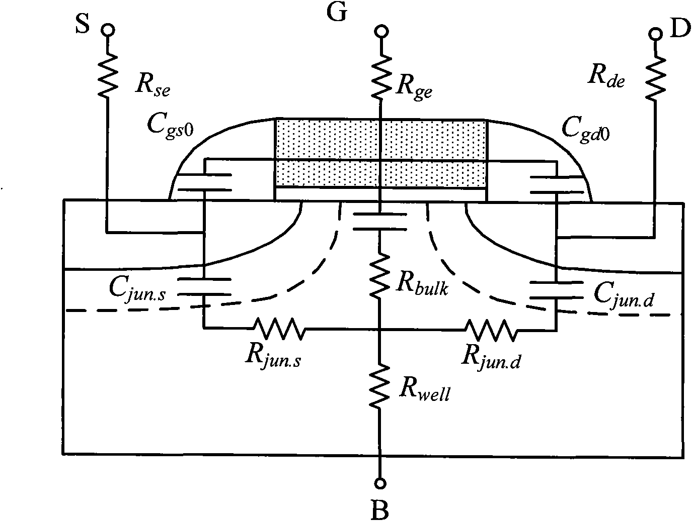
[0036] Such as figure 2 As shown, in order to establish a MOS transistor RF macro model, first establish a MOS transistor including gate, source, drain and substrate, and then establish gate node G, source node S, drain node D and substrate node B, and through the gate resistance R used to characterize the gate resistance of the MOS transistor ge Connect the gate to the gate node G, through the source resistance R used to characterize the source resistance of the MOS transistor se Connecting the source to ...


PUM


Abstract

The invention relates to an MOS (Metal Oxide Semiconductor) transistor radio frequency macro model establishing method which comprises the steps of: establishing an MOS transistor, a grid electrode node, a source electrode node, a drain electrode node and a substrate node, connecting a grid electrode to the grid electrode node by a grid resistor, connecting a source electrode to the source electrode node by a source resistor, and connecting a drain electrode to the drain electrode node through a drain resistor; establishing a source electrode junction capacitor, a drain electrode junction capacitor, a first substrate resistor, a second substrate resistor, a substrate bulk resistor and a substrate well resistor; and connecting the first substrate resistor, the second substrate resistor, the substrate bulk resistor and the substrate well resistor together by resistor network nodes. A simulation macro model obtained by the method of the invention has a four-resistor substrate network of a T-shaped structure; and by using the resistor substrate network, the utilization frequency of the MOS transistor radio frequency macro model can be ensured to be above 20 GHz, thereby greatly expanding the application frequency range of CMOS (Complementary Metal Oxide Semiconductor) radio frequency integrated circuit EDA (Electronic Design Automation) design.

Description

technical field [0001] The invention relates to the simulation of an integrated circuit, in particular, the invention relates to a method for establishing a radio frequency macro model of a MOS transistor. Background technique [0002] With the increasing application of CMOS technology in the radio frequency (RF) field, the accuracy of high frequency models of MOS devices is becoming more and more important for RF product design. Since the parasitic effects of MOS devices are more complex at high frequencies and have a greater correlation with the layout, the current practice is to build high-frequency models for MOS devices in the form of macro models. [0003] The BSIM3 SPICE model is an industry standard for CMOS models, figure 1 It is a "П" type three-resistor substrate network MOS transistor macro model in the prior art. where, through two capacitors (C SB and C DB ) and three resistors (R 1 , R 2 and R 3 ) to model the circuit. [0004] However, the MOS transis...

Claims


Application Information

Patent Timeline
IPC IPC(8): G06F17/50
Inventor 任铮吴华林胡少坚李曦石艳玲
Owner SHANGHAI INTEGRATED CIRCUIT RES & DEV CENT
Why Eureka
Try Eureka