Method and device for erasing nonvolatile memory

A non-volatile memory and erasing block technology, applied in the field of non-volatile memory erasing and non-volatile memory erasing devices, can solve the problems of VTT improvement and the impact of the overall performance of the memory, and achieve a good erasing effect. , the effect of improving the overall performance

Active Publication Date: 2010-12-22
GIGADEVICE SEMICON (BEIJING) INC
View PDF0 Cites 24 Cited by
  • Summary
  • Abstract
  • Description
  • Claims
  • Application Information

AI Technical Summary

Problems solved by technology

[0013] However, due to the erase operation with strong erase conditions, the V of the cell in the block will be T The distribution range is very wide, and the V of some cells T Too low, even lower than 0V
In this case, even through the soft programming operation, the V of these cells T will also be distributed over a large range of erased states, making it difficult to keep V T Increased to the programming state, which has a greater impact on the overall performance of the memory
And if the soft programming operation with strong programming conditions is adopted, it is very easy to change the V of the cell T raised above the upper limit of the normal erase state

Method used


Image

  • Method and device for erasing nonvolatile memory
  • Method and device for erasing nonvolatile memory
  • Method and device for erasing nonvolatile memory

Examples


Embodiment Construction

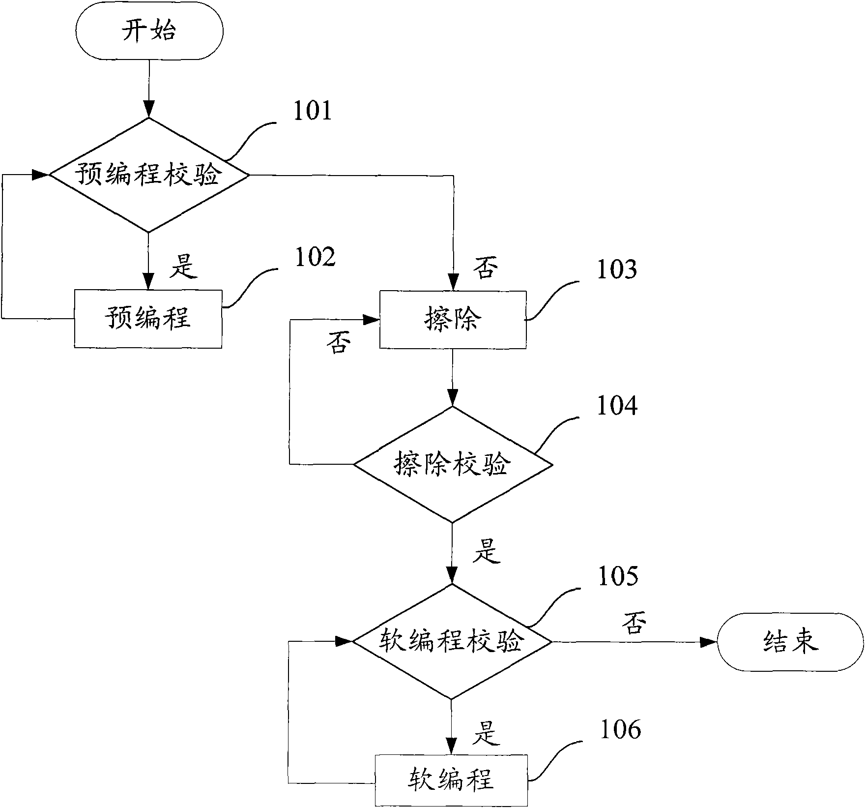
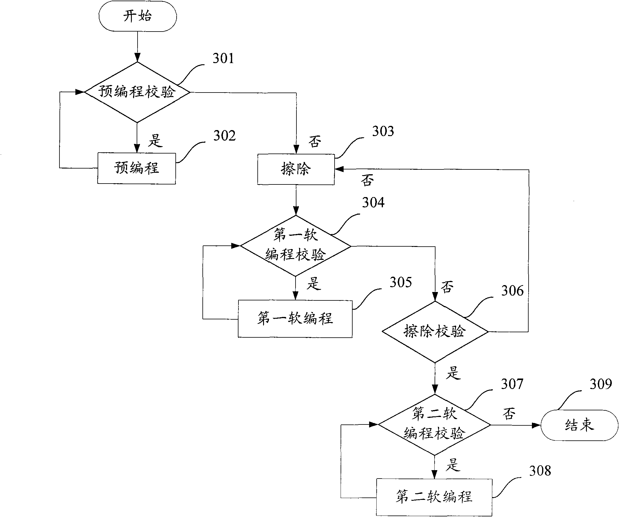
[0054] In order to make the above objects, features and advantages of the present invention more comprehensible, the present invention will be further described in detail below in conjunction with the accompanying drawings and specific embodiments.

[0055] In order for those skilled in the art to better understand the present invention, the following briefly introduces the composition principle of the non-volatile memory.

[0056] The non-volatile memory is composed of a storage unit (cell). The cell includes a capacitor and a transistor. The data in the cell depends on the charge stored in the capacitor, and the switch of the transistor controls the access of the data. Generally speaking, a cell may include a source (source, S), a drain (drain, D), a gate (gate, G), and a floating gate (floating gate, FG), and the FG may be connected to a voltage VG. If VG is a positive voltage, a tunnel effect is generated between FG and drain D, so that electrons are injected into FG, that...


PUM


Abstract

The invention discloses a method and a device for erasing a nonvolatile memory. The method comprises the following steps of: after an erasing step is executed, triggering a first soft programming step to converge a distribution range of a threshold value voltage of an erased memory unit once the existence of the erased memory unit in a target erasing block is detected by a first soft programming verification step; and after the successful erasure of the target erasing block is verified by an erasing verification step, if the erased memory unit which again appears in the target erasing block is detected by a second soft programming verification step, triggering a second soft programming step to program all the erased memory units in the target erasing block into a normal erasing range so as to render all the threshold value voltages in the memory units in an erased state. The method and the device can more precisely control VT of a cell after erasing operation, so that the subsequent program operation is facilitated and the whole performance of the memory is improved.

Description

technical field [0001] The invention relates to the technical field of semiconductor memory, in particular to a nonvolatile memory erasing method and a nonvolatile memory erasing device. Background technique [0002] With the rapid development and wide application of various electronic devices and embedded systems, such as computers, personal digital assistants, mobile phones, digital cameras, etc., there is a great need for a device that can be programmed many times, has a large capacity, is fast to read and write, and can be erased. Convenient, simple, less peripheral devices, low-cost non-volatile (can still maintain the stored data information in the case of power failure) storage device. The non-volatile memory device emerges as the times require under this background demand. [0003] To put it simply, a non-volatile memory is usually a MOS transistor, with a source (source), a drain (drain), a gate (gate), and a floating gate (floating gate, floating gate) ). It can...

Claims


Application Information

Patent Timeline
IPC IPC(8): G11C16/10G11C16/16G11C16/34
Inventor 舒清明潘荣华苏志强
Owner GIGADEVICE SEMICON (BEIJING) INC
Why Eureka
Try Eureka