Hole transport polymer for use in electronic devices

A technology for hole transport, organic electronic devices, applied in the field of hole transport polymers used in electronic devices

Inactive Publication Date: 2010-12-01
DYNAMIC ORGANIC LIGHT
View PDF0 Cites 23 Cited by
  • Summary
  • Abstract
  • Description
  • Claims
  • Application Information

AI Technical Summary

Problems solved by technology

Vapor deposition provides clear layer structures with excellent purity; however, this method is only applicable to low molecular weight molecules with high thermal stability [13]

Method used


Image

  • Hole transport polymer for use in electronic devices
  • Hole transport polymer for use in electronic devices
  • Hole transport polymer for use in electronic devices

Examples


Embodiment

[0073] The following examples are provided to illustrate some non-limiting embodiments of the invention. In each scheme, exemplary reactions and reagents are shown. Methods of synthesis of various compounds are known in the art.

[0074] plan 1

[0075]

[0076] Reactions and reagents used in the preparation of compound 5

[0077] 1a. NaH / DMF / 1-fluoro-4-nitrobenzene, reflux for 24 hours;

[0078] 1b. Sn / HCl / MeOH, reflux for 48 hours;

[0079] 1c. Methacrylic acid, DCC, DMAP, CH 2 Cl 2 ;with

[0080] 1d. VAZO88, toluene, chloroform, reflux for 24-48 hours.

[0081] Synthesis of 9-(4-nitrophenyl)-9H-carbazole (2)

[0082] Sodium hydride (1.85 g, 0.077 mol) was added to a solution of carbazole (11.70 g, 0.070 mol) in N,N-dimethylformamide (DMF) (100.0 ml) and the reaction mixture was heated under an atmosphere of dry nitrogen Stir at room temperature for 10 minutes. 1-Fluoro-4-nitrobenzene (7.53ml, 0.071mol) was added portionwise and the reaction mixture was heated...


PUM


Abstract

Organic light emitting diode (OLED) devices are one of the most promising alternatives to liquid crystal displays (LCDs) for flat panel display (FPD) applications. The OLED technique is based on organic semiconductors used either as hole- or electron transporting materials or as an emitter. Working on common problems of performance and life time in OLED preparation, improved charge transport molecules and polymers such as triarylamine- and poly(para-phenylene)- have been developed. Some useful materials include: (1) cyclic triarylamine-derivatives possessing enhanced glass transition temperatures; (2) triarylamine based low molecular mass hole-transport molecules and hole-transport polymers with pendant oxetane groups for processing out of solution and subsequent cross-linking; and (3) fluorenyl-segmented poly(para-phenylene)s with defined electrochemical properties. Provided is a polymer precursor that is useful as a hole transport polymer in OLED and other organic electronic devices.

Description

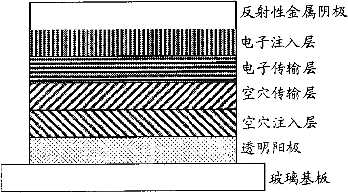
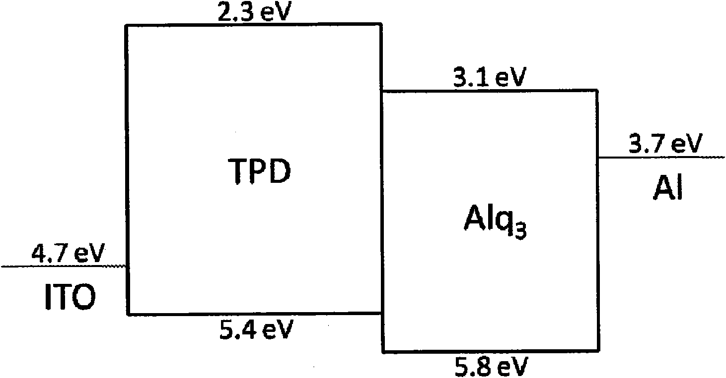
Background technique [0001] Organic Light Emitting Diodes (OLEDs) are currently being extensively investigated for many applications such as in the flat panel display industry, especially for applications requiring low power consumption, high color purity and long lifetime. The basic structure of a multilayer OLED was proposed by Eastman-Kodak in 1987 [3], and is based on electroluminescent and semiconducting organic materials packed between two electrodes, such as figure 1 shown in . Injecting charge from the electrode into the organic layer and performing charge transfer within each layer ( figure 2 ), electrons and electron-deficient (“holes”) can recombine to form excited singlet states. Then, as a result of the relaxation process, the singlet state is excited to emit light [1, 2]. [0002] To achieve high electroluminescence efficiency and long lifetime, the material must meet several specific requirements [4], including low injection barrier, balanced electron and ho...

Claims


Application Information

Patent Timeline
Patent Type & Authority Applications(China)
IPC IPC(8): C07D209/82
CPCC07D209/82H01L51/0059H01L51/0072H01L51/0081H01L51/004Y02E10/549H10K85/141H10K85/631H10K85/6572H10K85/324
Inventor 尼尔·高夫伊桑·蔡威廉·A·赫夫曼克里斯托弗·D·威廉斯阿里莱尼·A·达默龙
Owner DYNAMIC ORGANIC LIGHT
Why Eureka
Try Eureka