High frequency plasma CVD apparatus, high frequency plasma CVD method and semiconductor thin film manufacturing method

A high-frequency plasma, plasma technology, applied in the ion CVD method. , In the field of ion CVD method, it can solve the problems of difficult uniform film formation, breakdown, leakage current, etc., and achieve the effect of good Raman spectral characteristics

Inactive Publication Date: 2010-11-24
村田 正义
View PDF2 Cites 0 Cited by
  • Summary
  • Abstract
  • Description
  • Claims
  • Application Information

AI Technical Summary

Problems solved by technology

[0050] In addition, Patent Document 5 points out that in conventional plasma CVD apparatuses using parallel plate electrodes and plasma CVD apparatuses using trapezoidal electrodes, leakage currents, abnormal discharges, or Breakdown occurs, and plasma is generated in places other than a pair of electrodes, making it difficult to form a uniform film

Method used


Image

  • High frequency plasma CVD apparatus, high frequency plasma CVD method and semiconductor thin film manufacturing method
  • High frequency plasma CVD apparatus, high frequency plasma CVD method and semiconductor thin film manufacturing method
  • High frequency plasma CVD apparatus, high frequency plasma CVD method and semiconductor thin film manufacturing method

Examples


Embodiment 1

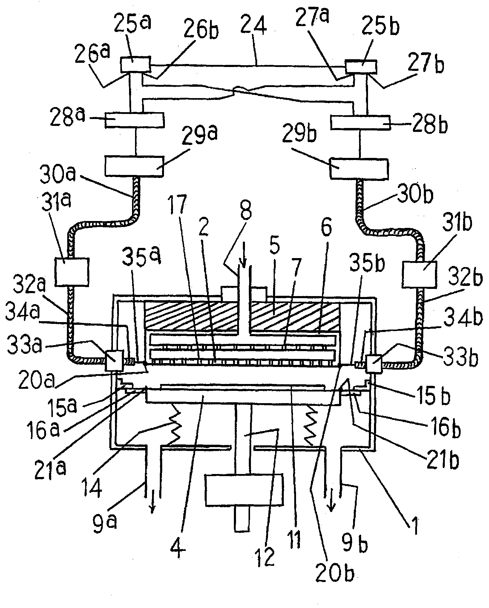
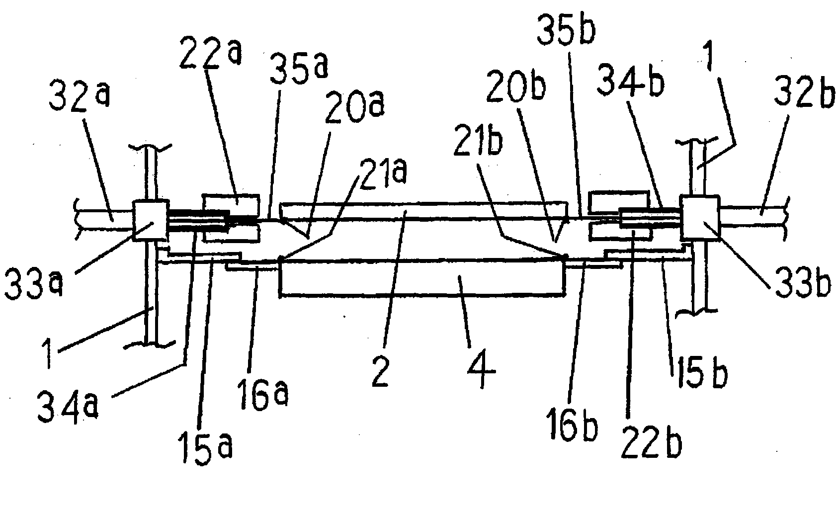
[0247] First, refer to Figure 1 to Figure 8 The plasma CVD apparatus and the plasma CVD method related to the first embodiment of the present invention will be described.

[0248] figure 1 It is a schematic diagram showing the whole plasma CVD apparatus related to the first embodiment of the present invention; figure 2 is to figure 1 An explanatory diagram of the structure of a power supply unit that supplies power to a pair of electrodes inside the plasma CVD apparatus shown; image 3 is to figure 1 A conceptual diagram of propagation of electric power supplied by a pair of electrodes inside the plasma CVD apparatus shown; Figure 4 is indicated by using figure 1 An explanatory diagram of an example of a method of adjusting power transmission when forming an i-type microcrystalline silicon film in the plasma CVD apparatus shown and performing power supply; Figure 5 is from figure 1 An explanatory diagram of a typical example of the pulse-modulated output output...

Embodiment 2

[0456] Next, refer to Figure 9 to Figure 11 A plasma CVD apparatus and a plasma CVD method related to the second embodiment of the present invention will be described.

[0457] Figure 9 It is a schematic diagram showing the whole of the plasma CVD apparatus related to the second embodiment of the present invention, Figure 10 is for figure 2 An explanatory diagram of a power supply device that supplies power to a pair of electrodes using a balun inside the plasma CVD apparatus shown, Figure 11 yes Figure 10 The shown conceptual diagram shows the flow of high-frequency current at a power supply device that supplies power to a pair of electrodes using a balun.

[0458] First, the configuration of the device will be described. However, the same reference numerals are assigned to the same components as those shown in the plasma CVD apparatus related to the first embodiment of the present invention described above, and description thereof will be omitted.

[0459] First,...


PUM

PropertyMeasurementUnit
thicknessaaaaaaaaaa
sizeaaaaaaaaaa
thicknessaaaaaaaaaa

Abstract

Provided are large area and uniform VHF plasma CVD apparatus and method wherein a plasma generating source constitutes the VHF plasma CVD apparatus for manufacturing a tandem-type thin film silicon solar cell, and influences of standing waves, generation of harmful plasma other than between a pair of electrodes and supply power consumption other than between the pair of electrodes are suppressed. First and second power feed points are arranged on an electrode at positions facing each other. A distance between the power feed points is set at an integral multiple of a half of the wavelength of the using power, and a pulse power separated interms of time is supplied. The pulse power is outputted from two phase-variable double output high frequency power supplies which can perform pulse modulation. Thus, a first standing wave wherein the anti-node position accords with the positions of the first and the second power feed points, and a second standing wave wherein the node position accords with the positions of the first and the second power feed points are alternately generated in terms of time.

Description

technical field [0001] The present invention relates to a high-frequency plasma CVD device, a high-frequency plasma CVD method and a semiconductor thin-film manufacturing method used in the manufacture of an integrated tandem-type thin-film solar battery module. In particular, it relates to a VHF plasma CVD apparatus with a frequency of 30 MHz to 300 MHz (VHF band) and a VHF plasma CVD method. [0002] Also, it relates to a high-frequency plasma CVD apparatus and a high-frequency plasma CVD method used in the manufacture of various devices to which microcrystalline silicon films and quasicrystalline silicon films are applied. Background technique [0003] A multi-junction photoelectric conversion element in which a plurality of semiconductor photoelectric conversion units having a photoelectric conversion function are stacked is very effective in improving power conversion efficiency by combining top and bottom cells with different wavelength absorption bands, for example, i...

Claims


Application Information

Patent Timeline
Patent Type & Authority Applications(China)
IPC IPC(8): H01L21/205C23C16/505
CPCC23C16/24C23C16/509H01J37/32091
Inventor 村田正义
Owner 村田 正义
Why Eureka
Try Eureka