
Evaluation method of influence of optical element surface waviness on laser damage threshold and method for obtaining element optimal processing parameters therefrom

A technology of laser damage threshold and surface waviness, which is applied in the direction of optical components, optics, and testing optical performance, can solve problems such as inaccurate results and achieve high processing quality

Inactive Publication Date: 2010-11-17
HARBIN INST OF TECH
View PDF1 Cites 10 Cited by
  • Summary
  • Abstract
  • Description
  • Claims
  • Application Information

AI Technical Summary

Problems solved by technology

[0003] The purpose of the present invention is to solve the problem that there is currently no method for evaluating the degree of influence of the surface waviness of the optical element on the laser damage threshold of the optical element, and the problem of inaccurate results in the method for obtaining the optimal processing parameters of the element. , providing a method for evaluating the influence of optical element surface waviness on its laser damage threshold and a method for obtaining the optimal processing parameters of the element

Method used


Image

  • Evaluation method of influence of optical element surface waviness on laser damage threshold and method for obtaining element optimal processing parameters therefrom
  • Evaluation method of influence of optical element surface waviness on laser damage threshold and method for obtaining element optimal processing parameters therefrom
  • Evaluation method of influence of optical element surface waviness on laser damage threshold and method for obtaining element optimal processing parameters therefrom

Examples


specific Embodiment approach 1

[0018] Specific implementation mode one : the evaluation method of the influence of the surface waviness of the optical element of the present embodiment on its laser damage threshold, its process is as follows:

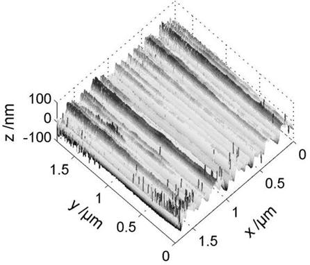
[0019] Step 1. Obtain the shape data matrix of the original processed surface of the optical element by using the detection instrument;

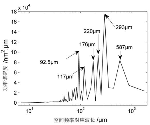
[0020] Step 2. According to the morphology data matrix obtained in step 1, the power spectral density curve of the original processed surface of the optical element is obtained, and then each characteristic frequency and the amplitude of each characteristic frequency of the original processed surface of the optical element are obtained;

[0021] Step 3. For each characteristic frequency obtained in step 2, use the two-dimensional continuous wavelet transform method to extract and reproduce the three-dimensional shape of each characteristic frequency, and use the Fourier mode method to calculate the light intensity distribution ins...

specific Embodiment approach 2

[0025] Specific implementation mode two: This embodiment is a further description of the evaluation method of the influence of the surface waviness of the optical element on its laser damage threshold in the first embodiment. The specific process of the content described in step two is:

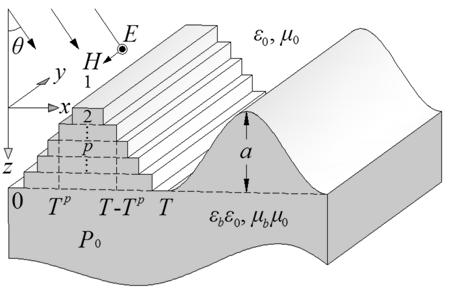
[0026] make z ( x ) represents the topography data matrix of the original processed surface of the optical element obtained in step 1, where z ( x ) contains N data points, and every two adjacent data points have the same sampling interval Δ x , the overall sampling length is L = N Δ x ;

[0027] The power spectral density is defined as the square of the Fourier spectrum amplitude of each frequency component of the wavefront, which is the result of Fourier transforming the surface profile function of the optical element in the space domain in the frequency domain, and its one-dimensional definition is ,in, ν is the spatial frequency, Δ ν is the frequency interval, A ( ν ) is t...

specific Embodiment approach 3

[0035] Specific implementation mode three: This embodiment is a further description of the evaluation method of the influence of the surface waviness of the optical element on its laser damage threshold in the first or second embodiment. The specific process of the content described in step three is:

[0036] The general form of two-dimensional continuous wavelet transform (CWT2D, ContinuousWaveletTransform2D) is:

[0037] ,

[0038] in, is the plane Cartesian coordinates, represents a two-dimensional signal, Represents a two-dimensional continuous wavelet transform, yes , displacement in the direction, , superscripts in expressions T means transpose, is the scale factor, is the coordinate rotation factor, is the counterclockwise rotation angle of the coordinate system, Represents the two-dimensional basic wavelet function The scaling, coordinate rotation and two-dimensional displacement of the for the conjugate;

[0039] Eigenfrequency f s...


PUM


Abstract

The invention relates to an evaluation method of influence of an optical element surface waviness on a laser damage threshold and a method for obtaining optimal processing parameters of the element therefrom, in particular to a method for evaluating surface quality of an optical element and a method for obtaining the optimal processing parameters of the element. The evaluation method comprises the following steps of obtaining a morphology data matrix of an original processing surface; obtaining a relative laser damage threshold relevant to each characteristic frequency by utilizing a power spectrum density method, a two-dimensional continuous wavelet transformation method and a fourier modulus method; and selecting a minimum value as an evaluation result. In the method for obtaining the optimal processing parameters of the optical element, the optimal processing parameters are obtained by utilizing the evaluation method and comparing the relative laser damage thresholds of thr optical element obtained under various processing parameter conditions. The invention can be used for evaluating the quality of the optical element and can also be used for guiding the processing process of the optical element.

Description

technical field [0001] The invention relates to a method for evaluating the surface quality of an optical element and a method for obtaining the optimum processing parameters of the element. Background technique [0002] Fusion energy is clean, pollution-free and almost inexhaustible. It is an ideal way to solve energy problems in the future. At present, all developed countries attach great importance to it. The high-power solid-state laser driver required to control nuclear fusion with laser needs to provide high energy when irradiating the nuclear target pellet in the final stage to achieve nuclear fusion ignition (the energy required for ignition is 3-10MJ / cm 2 , 3 ~ 5ns). However, due to the relatively low laser damage threshold of various strong light optical components used in current laser drivers (for example, the actual threshold of KDP crystal is 12~20J / cm 2 , 1ns), which greatly limits the energy output of ultra-high-power solid-state lasers, making it difficult...

Claims


Application Information

Patent Timeline
IPC IPC(8): G02B27/00G01M11/02G01B21/30
Inventor 梁迎春陈明君李明全姜伟王健许乔
Owner HARBIN INST OF TECH
Learn More