Solid-state imaging device and imaging apparatus

A technology for solid-state imaging devices and semiconductors, which is applied in the manufacturing of electric solid-state devices, semiconductor devices, and semiconductor/solid-state devices, etc., can solve the problems of actual sensitivity changes of photoelectric conversion units, and achieve the effect of improving the actual sensitivity.

Inactive Publication Date: 2010-10-27
SONY SEMICON SOLUTIONS CORP
View PDF8 Cites 4 Cited by
  • Summary
  • Abstract
  • Description
  • Claims
  • Application Information

AI Technical Summary

Problems solved by technology

[0019] Therefore, when the incident angle of light is shifted only slightly,...

Method used


Image

  • Solid-state imaging device and imaging apparatus
  • Solid-state imaging device and imaging apparatus
  • Solid-state imaging device and imaging apparatus

Examples


Embodiment Construction

[0043] Embodiments of the present invention will be described below with reference to the drawings. Instructions are given in the following order:

[0044] 1. The structure of the camera device;

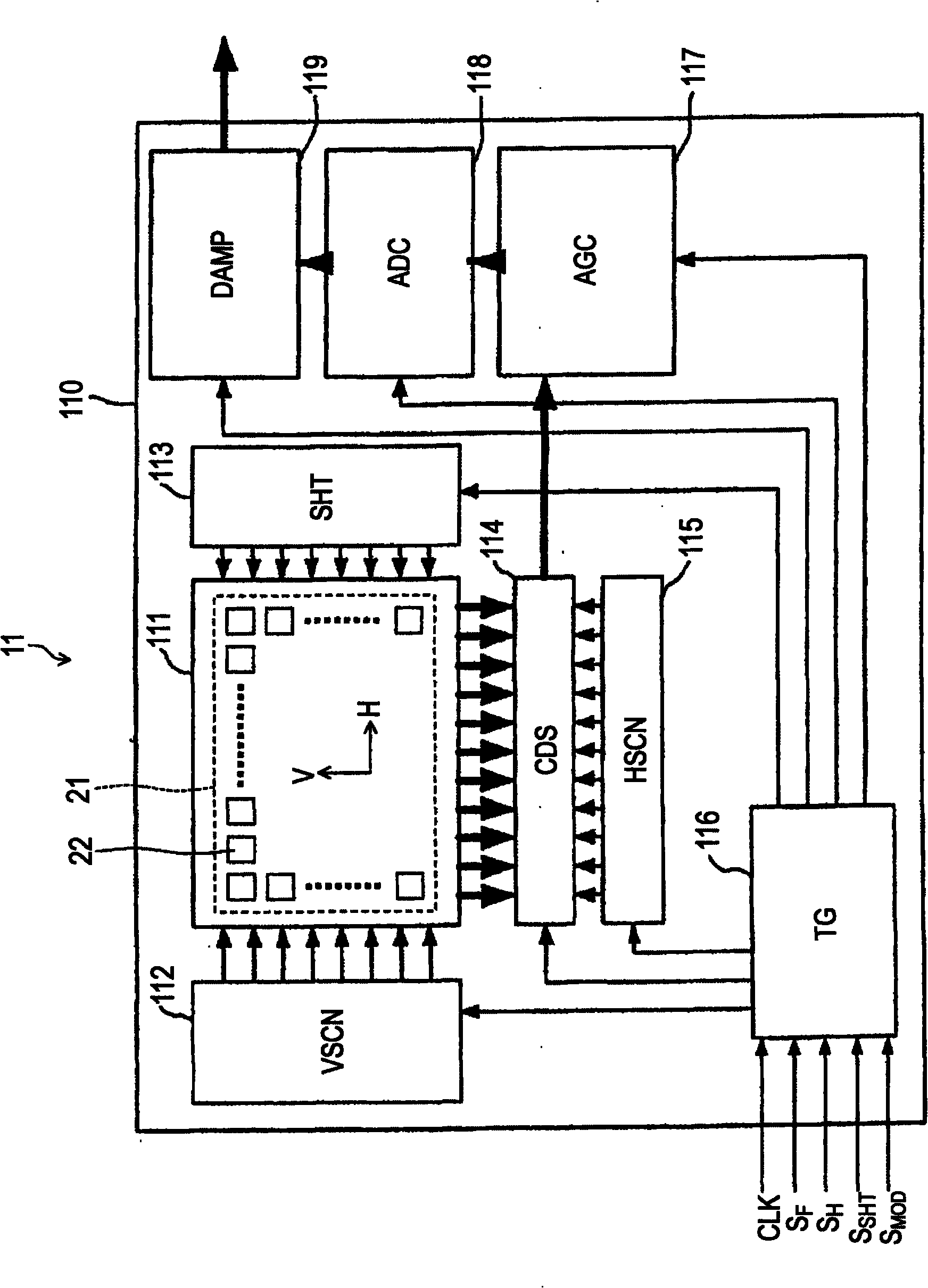
[0045] 2. The structure of solid-state imaging devices;

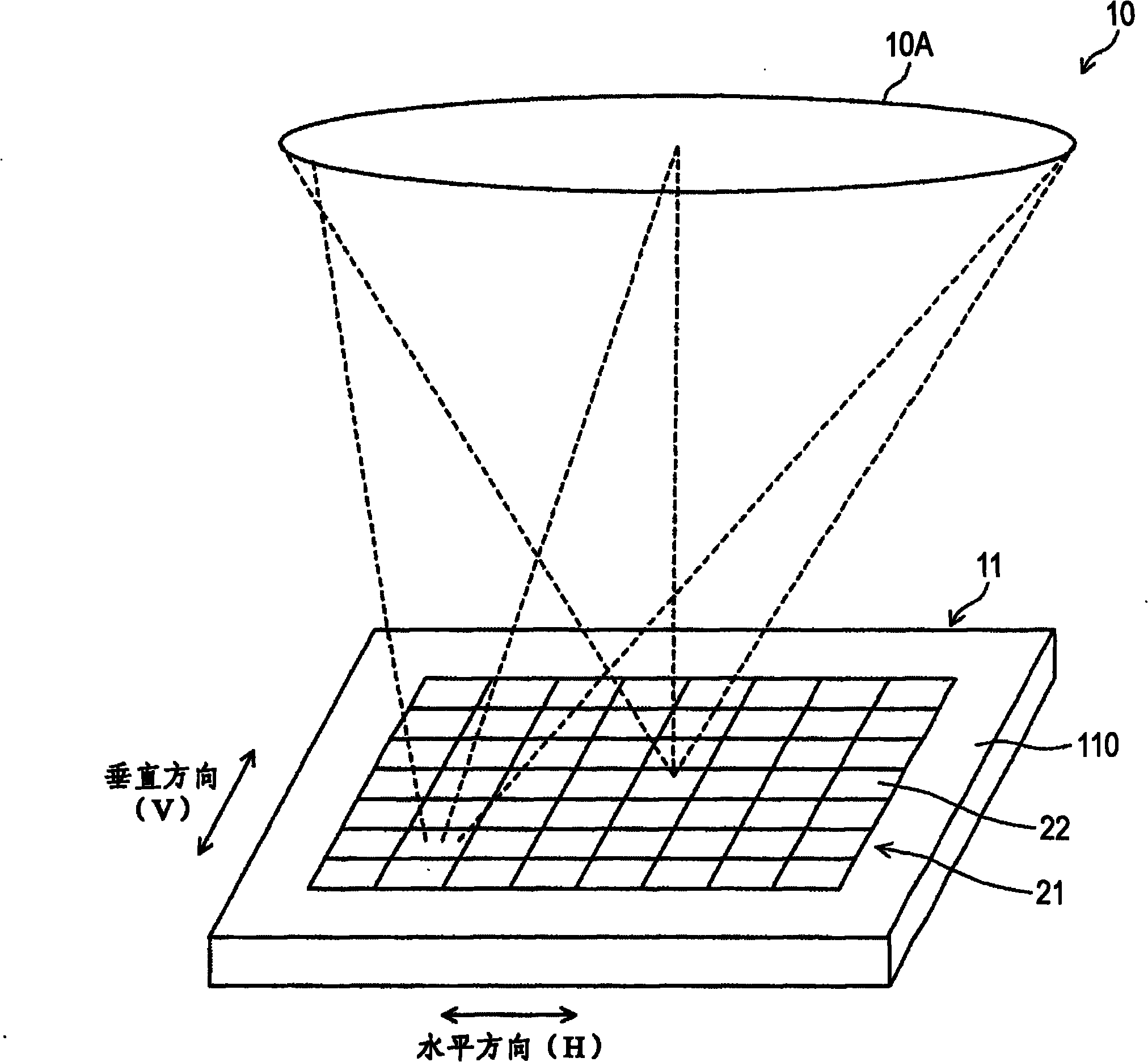
[0046] 3. Various wirings in the light receiving unit and the layout of the photoelectric conversion unit;

[0047] 4. The section of the wiring part;

[0048] 5. The wiring body shape of the wiring section; and

[0049] 6. Operation of camera device

[0050] Structure of the imaging device 1

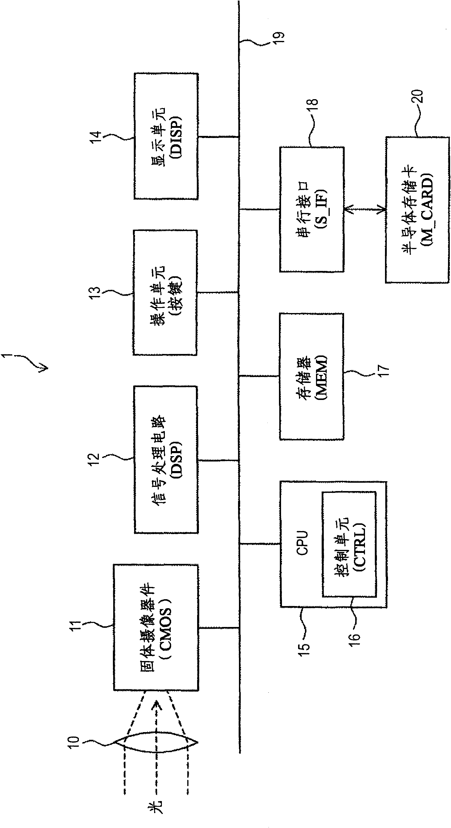
[0051] figure 1 is a block diagram of the imaging device 1 according to the embodiment of the present invention.

[0052]The imaging device 1 includes an optical unit 10 , a solid-state imaging device (CMOS) 11 , a signal processing circuit (DSP) 12 , an operation unit (key) 13 , and a display unit (DISP) 14 . Furthermore, the imaging device 1 includes a central processing unit (Central Processing Unit, CPU) 15, a memory (MEM)...


PUM


Abstract

A solid-state imaging device includes: a semiconductor substrate; photoelectric conversion units formed in array on the semiconductor substrate and forming a light receiving unit; and wiring sections formed in positions among the photoelectric conversion units. The wiring sections include wiring bodies formed by superimposing wiring layers on the light receiving unit and including a bottom wiringbody on the semiconductor substrate side, a top wiring body on an uppermost side, and an intermediate wiring body between the bottom wiring body and the top wiring body, and contacts connecting the wiring bodies in order of vertical overlap, and in at least one of the wiring sections, the wiring bodies other than the bottom wiring body are superimposed while being shifted from a position right above the bottom wiring body, and amounts of shift of the intermediate wiring body and the contacts connected to the intermediate wiring body are the same.

Description

[0001] Cross References to Related Applications [0002] This application contains subject matter related to the disclosure of Japanese Priority Patent Application JP 2009-103176 filed in the Japan Patent Office on Apr. 21, 2009, the entire content of which is hereby incorporated by reference. technical field [0003] The present invention relates to a solid-state imaging device and an imaging device including a wiring portion formed in a light receiving unit in which a plurality of photoelectric conversion units are arranged. Background technique [0004] JP-A-2003-273342 (Patent Document 1) and JP-A-2003-264281 (Patent Document 2) disclose solid-state imaging devices. [0005] In a solid-state imaging device, a plurality of photoelectric conversion units are two-dimensionally arranged in a light-receiving unit of a semiconductor substrate. [0006] A plurality of wiring portions are formed on the light receiving unit of the semiconductor substrate, extending along a prede...

Claims


Application Information

Patent Timeline
IPC IPC(8): H01L27/146H04N5/335H04N5/225H01L21/768H01L23/522H01L27/14
CPCH01L27/14636H04N5/374H04N5/335H01L27/14632H01L27/14605H04N25/00H04N25/76
Inventor 佐藤公彦
Owner SONY SEMICON SOLUTIONS CORP
Why Eureka
Try Eureka