Light-emitting device and illumination apparatus
一种发光装置、发光元件的技术,应用在照明装置、照明装置的零部件、电致发光光源等方向,达到紧凑且低价格化、防止闪烁的效果
- Summary
- Abstract
- Description
- Claims
- Application Information
AI Technical Summary
Problems solved by technology
Method used
Image

Examples
no. 1 Embodiment approach
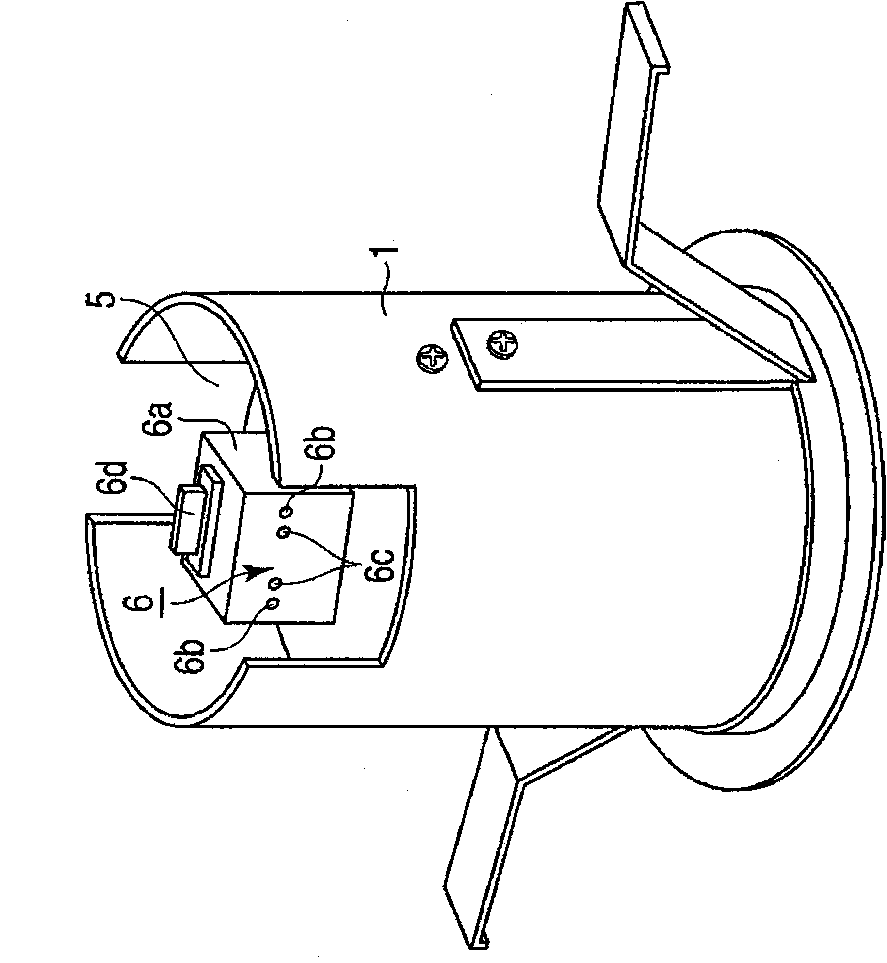
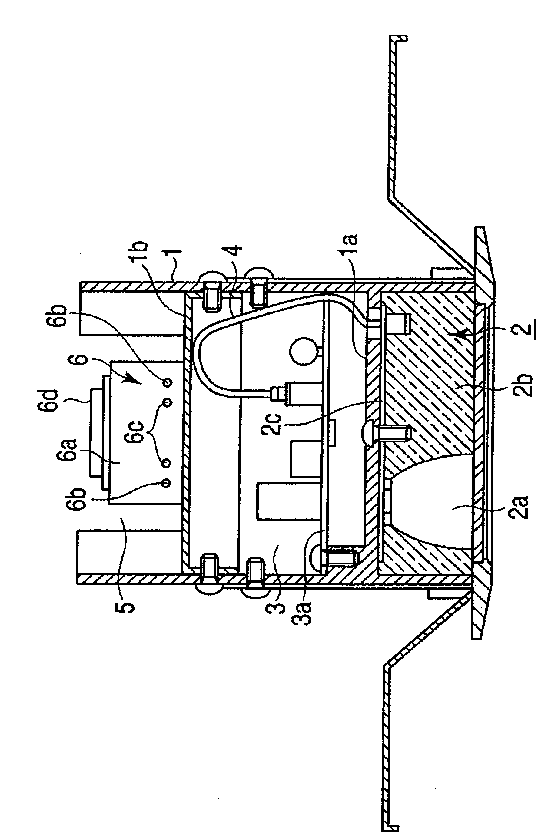
[0078] First, the lighting device of the present invention will be briefly described. exist figure 1 as well as figure 2 Among them, 1 is the frame body of the device body, and the frame body 1 is made of aluminum die-casting (die-cast), and has a cylindrical shape with both ends open. The housing 1 is vertically divided into three by partition members 1 a and 1 b , and a space between the lower opening and the partition member 1 a is formed in the light source unit 2 . In this light source part 2, several LED2a and reflector 2b which are semiconductor light emitting elements are provided. The some LED2a is arrange|positioned at equal intervals along the circumferential direction of the disk-shaped wiring board 2c provided in the lower surface of the partition member 1a, and is mounted.
[0079] A space between the partition members 1 a and 1 b of the frame body 1 is formed in the power source compartment 3 . In the power supply chamber 3, a wiring board 3a is disposed o...
Deformed example 1
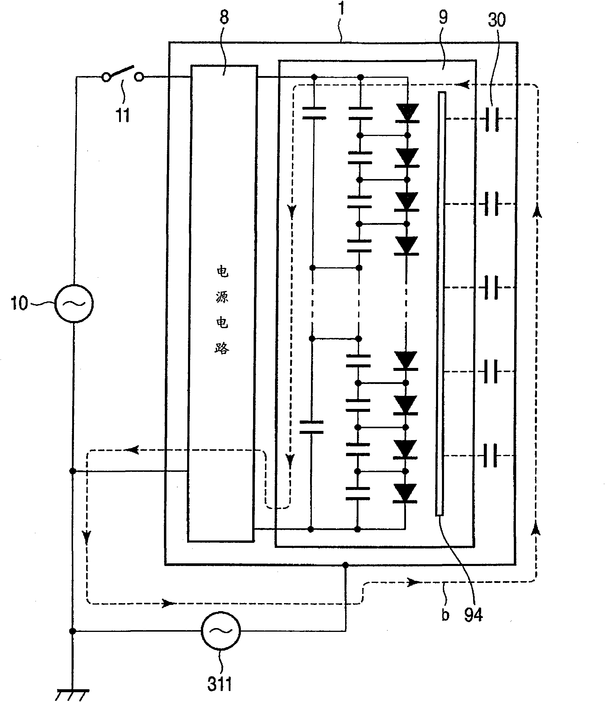
[0100] Figure 6 A modified example of the LED module described in the first embodiment is shown.
[0101] In this case, the LED module 31 is configured by connecting a plurality of (six in the illustrated example) LED elements 311a to 311f in series, and connecting the series circuit between the positive and negative lines 31a and 31b output by the DC power supply. First bypass capacitors 312a to 312f are connected in parallel to these LED elements 311a to 311f, respectively. Furthermore, the second bypass capacitor 313a is connected in parallel to the series circuit of the LED elements 311b to 311f, the second bypass capacitor 313b is connected in parallel to the series circuit of the LED elements 311c to 311f, and the LED elements 311e to 311f are connected in parallel. The second bypass capacitor 313c is connected in parallel to the series circuit. These second bypass capacitors 313a, 313b, and 313c can make the connection points B1, C1, and D1 of the series circuit of t...
Deformed example 2
[0104] Figure 7 Another modified example of the LED module described in the first embodiment is shown.
[0105] At this time, the LED module 32 is as follows Figure 7As shown, a plurality of (six in the illustrated example) LED elements 321a to 321f are connected in series, and the series circuit is connected between the positive and negative lines 32a and 32b of the DC power output. First bypass capacitors 322a to 322f are connected in parallel to these LED elements 311a to 311f, respectively. Furthermore, the second bypass capacitor 323a is connected in parallel to the series circuit of the LED elements 321b to 321e, and the second bypass capacitor 323b is connected in parallel to the series circuit of the LED elements 321d and 321e. These second bypass capacitors 323a and 323b can make each connection point B2 of the series circuit of the LED elements 321a to 321f when the negative side line 32b of the LED elements 321a to 321f is set as the ground point A2 and this gro...
PUM
 Abstract
Description
Claims
Application Information
 - R&D
- Intellectual Property
- Life Sciences
- Materials
- Tech Scout
- Unparalleled Data Quality
- Higher Quality Content
- 60% Fewer Hallucinations
Browse by: Latest US Patents, China's latest patents, Technical Efficacy Thesaurus, Application Domain, Technology Topic, Popular Technical Reports.
© 2025 PatSnap. All rights reserved.Legal|Privacy policy|Modern Slavery Act Transparency Statement|Sitemap|About US| Contact US: help@patsnap.com