Photoelectric conversion device and manufacturing method of the same
A technology for photoelectric conversion elements and manufacturing methods, which is applied in the fields of electrical components, photovoltaic power generation, and final product manufacturing, etc., can solve problems such as the range of cumbersome manufacturing conditions in the manufacturing process, large performance deviation of photoelectric conversion elements, and poor productivity and economy. Excellent versatility, improved process tolerance, improved productivity and improved economy
- Summary
- Abstract
- Description
- Claims
- Application Information
AI Technical Summary
Problems solved by technology
Method used
Image
Examples
Embodiment 1
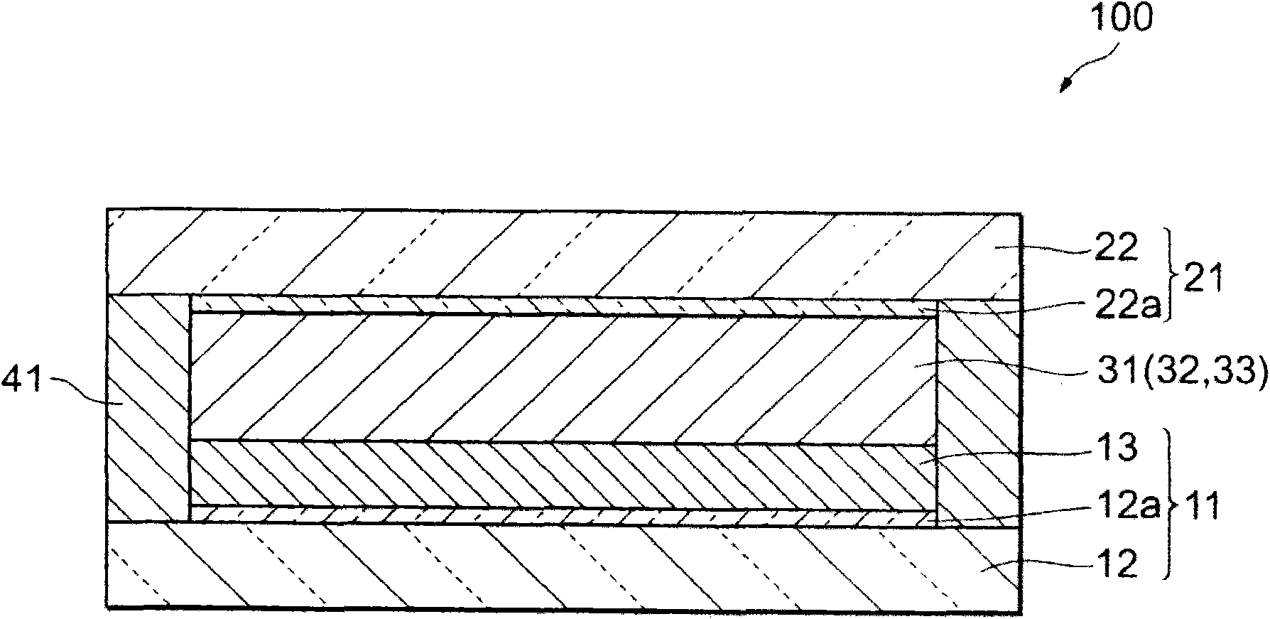
[0083] First, prepare a transparent glass substrate (manufactured by Asahi Glass Fabritec Co., Ltd.) with fluorine-doped SnO as a transparent conductive film, and screen-print a commercially available titanium oxide paste (particle size 18 nm), heated at 60°C for 10 minutes to dry the paste, and then fired at 450°C for 30 minutes to produce a titanium oxide film with a thickness of about 3 µm. Subsequently, adjust the ethanol solution of N719 pigment (pigment concentration: 3×10 -4 M) As a dye-adsorbing solution, the above-mentioned titanium oxide thin film was immersed in the dye-adsorbing solution at room temperature for 8 hours to perform a dye-adsorbing treatment, and then washed with ethanol and vacuum-dried to prepare a dye-loaded metal oxide layer , thus obtaining the working electrode.
[0084] Subsequently, commercially available carbon black (N 2 The specific surface area is 315m 2 / g), the electrolyte (pseudo-solid electrolyte) was prepared by kneading. The cont...
Embodiment 2
[0088] Except for using a glass fiber screen (manufactured by Clever Co., Ltd., the number of meshes per 1 inch square is 16, the mesh size is about 1 mm, and the thickness is 230 μm) as the mesh-shaped support member, other uses are the same as in Example 1. The electrolyte sheet of Example 2 (thickness is about 240 μm) was produced, and, except for using the electrolyte sheet of Example 2, other methods were processed in the same way as in Example 1, and a total of 5 samples of Example 2 were obtained. Photoelectric conversion element.
PUM
| Property | Measurement | Unit |
|---|---|---|
| thickness | aaaaa | aaaaa |
| particle diameter | aaaaa | aaaaa |
| thickness | aaaaa | aaaaa |
Abstract
Description
Claims
Application Information
 - Generate Ideas
- Intellectual Property
- Life Sciences
- Materials
- Tech Scout
- Unparalleled Data Quality
- Higher Quality Content
- 60% Fewer Hallucinations
Browse by: Latest US Patents, China's latest patents, Technical Efficacy Thesaurus, Application Domain, Technology Topic, Popular Technical Reports.
© 2025 PatSnap. All rights reserved.Legal|Privacy policy|Modern Slavery Act Transparency Statement|Sitemap|About US| Contact US: help@patsnap.com


