
Liquid crystal display device

A liquid crystal display device and transistor technology, which is applied to static indicators, instruments, etc., can solve problems such as the gate driver 106 being unable to perform normal logic operations, and the noise of the boot screen.

Inactive Publication Date: 2010-09-08
AU OPTRONICS CORP
View PDF3 Cites 12 Cited by
  • Summary
  • Abstract
  • Description
  • Claims
  • Application Information

AI Technical Summary

Problems solved by technology

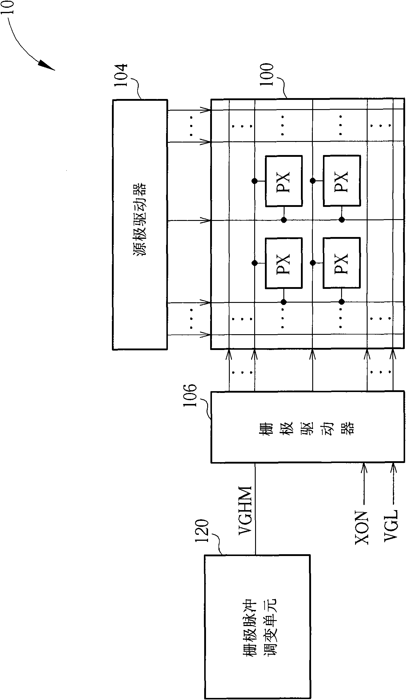
However, within a predetermined period of time after the liquid crystal display device 10 is powered on, during the operation of the gate pulse modulating unit 120 with the waveform shaving function, the clamping voltage used to provide the waveform shaving function can be quickly increased to Micro Motion bit and fed into the gate driver 106, but at this time the low-level gate signal reference voltage VGL has not yet established an operating level, so the gate driver 106 cannot perform normal logic operations, thus generating complex noise-like gates Signal
And because the reset signal XON at this time will enable the gate driver 106 to output all gate signals to the pixel array unit 100 at the same time, that is, the complex noise-like gates generated by the gate driver 106 within a predetermined period after power-on. All the signals will be fed into the pixel array unit 100, which will cause noise phenomenon in the boot screen

Method used


Image

  • Liquid crystal display device
  • Liquid crystal display device
  • Liquid crystal display device

Examples


Embodiment Construction

[0030] Hereinafter, specific embodiments of the liquid crystal display device according to the present invention will be described in detail with the accompanying drawings, but the provided embodiments are not intended to limit the scope of the present invention.

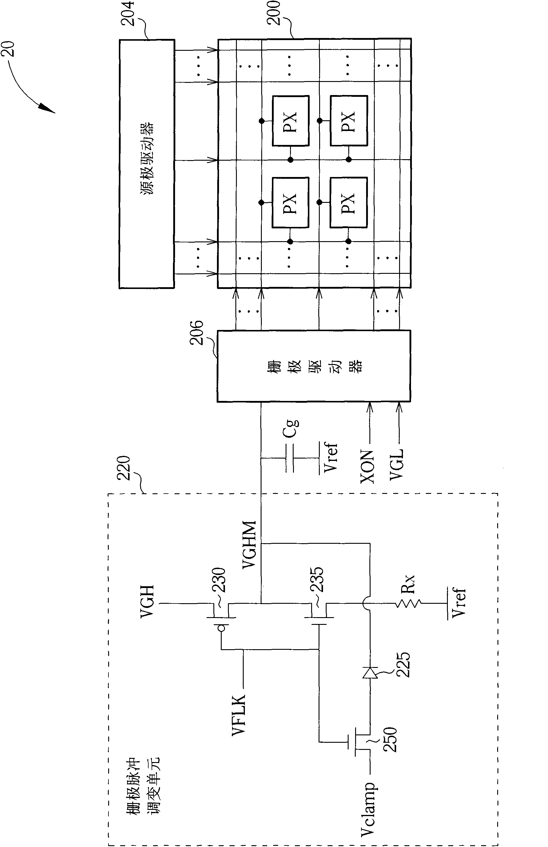
[0031] figure 2 It is a structural schematic diagram of the first embodiment of the liquid crystal display device of the present invention. Such as figure 2 As shown, the liquid crystal display device 20 includes a pixel array unit 200 having a plurality of pixels PX, a source driver 204 , a gate driver 206 , a capacitor Cg, and a gate pulse modulation unit 220 . The source driver 204 is used to provide complex data signals to the pixel array unit 200 . The gate driver 206 is used to modulate the voltage VGHM and the low-level gate signal reference voltage VGL according to the high-level gate signal to provide complex gate signals to the pixel array unit 200, and the pixel array unit 200 is based on the complex ...


PUM


Abstract

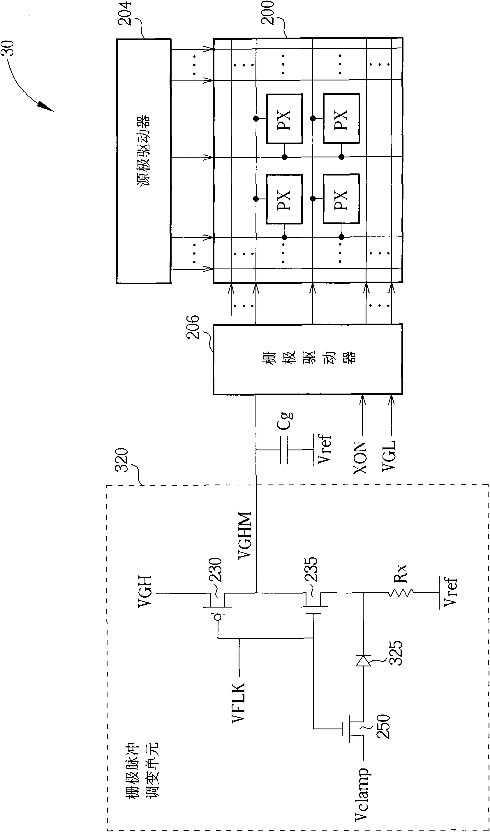
The invention relates to a liquid crystal display device. The device comprises a source driver for providing a plurality of data signals, a grid driver for modulating a voltage according to a high level grid signal to provide a plurality of grid signals, a pixel array unit for displaying images according to the plurality of data signals and the plurality of grid signals, and a grid pulse modulating unit. The grid pulse modulating unit comprises a waveform chamfering circuit, a diode and a transistor. The waveform chamfering circuit is used for providing a high level grid signal modulating voltage according to a chamfering control signal and a reference voltage of the high level grid signal so as to execute a waveform chamfering operation on the plurality of grid signals. The waveform chamfering operation has a voltage clamping function according to the unidirectional transmission property of the diode, and the transistor enables / removes the voltage clamping function according to the chamfering control signal.

Description

technical field [0001] The invention relates to a liquid crystal display device, in particular to a liquid crystal display device capable of avoiding the phenomenon of noise in the boot screen. Background technique [0002] Liquid crystal display (Liquid Crystal Display; LCD) has the advantages of light and thin appearance, power saving and low radiation, so it has been widely used in computer screens, mobile phones, personal digital assistants (PDAs), flat-screen TVs, and other communication / Electronic products such as entertainment equipment. The working principle of the liquid crystal display device is to change the arrangement state of the liquid crystal molecules in the liquid crystal layer by changing the voltage difference between the two ends of the liquid crystal layer, thereby changing the light transmittance of the liquid crystal layer, and then cooperate with the light source provided by the backlight module to display images. figure 1 It is a schematic diagram...

Claims


Application Information

Patent Timeline
IPC IPC(8): G09G3/36
Inventor 李建锋郑晓钟徐兆庆
Owner AU OPTRONICS CORP
Learn More