Single crystal thin film of organic semiconductor compound and method for producing the same
一种有机半导体、单晶薄膜的技术,应用在半导体器件、化学仪器和方法、半导体/固态器件制造等方向,能够解决出现缺陷、不可能稳定地制备大面积和均匀的单晶薄膜等问题
- Summary
- Abstract
- Description
- Claims
- Application Information
AI Technical Summary
Problems solved by technology
Method used
Image
Examples
preparation example Construction
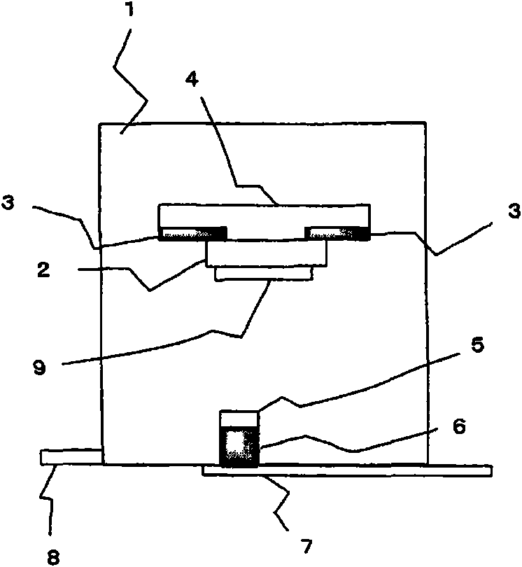
[0080] figure 1 is a schematic diagram illustrating an example of a thin film production apparatus. Such as figure 1 Shown, the preparation device 1 of thin film is made up of following: be used for the base 4 of fixed substrate 2, be used for heating the heater 7 of the sublimation crucible 5 that places organic semiconductor compound (organic semiconductor material) 6, and make the preparation device of thin film The internal pressure of 1 reaches the exhaust port 8 of the vacuum state. In order to control the temperature of the substrate 2, a Peltier device 3 is preferably fixed on a susceptor 4, as shown.
[0081] First, the substrate 2 prepared by forming an organic solvent liquid film (oil film) 9 by applying a specific organic solvent on the substrate 2 is set on the susceptor 4 in the thin film manufacturing apparatus 1 . On the other hand, the organic semiconductor compound 6 is placed in the sublimation crucible 5, and the sublimation crucible 5 is placed at a pre...
Embodiment 1
[0095] ITO (which is transparent electrode) glass substrate (10 mm square, produced by EHC), and an organic solvent liquid film having a thickness of 10 μm was prepared. Place the glass substrate on which the organic solvent liquid film is formed in the chamber of the vacuum vapor deposition device.
[0096] Then, rubrene (manufactured by Sigma Aldrich Japan) was placed in a sublimation crucible, followed by vacuum vapor deposition for 2 hours. In this vapor deposition, the conditions are: vacuum degree 1×10 -3 Pa, the heating temperature of the heater is 180° C., and the vapor deposition rate is 5 nm / min. During this treatment, the temperature of the glass substrate was 25°C.
[0097] The obtained glass substrate with the organic solvent liquid film was taken out from the chamber and observed with a microscope to confirm that a rubrene single crystal thin film was formed on the glass substrate. The obtained single crystal was approximately circular, with an average diamet...
Embodiment 2
[0099] A rubrene single crystal thin film was prepared in the same manner as in Example 1, except that the temperature of the glass substrate with ITO was changed to -10°C.
[0100] Microscopic observation of the obtained single crystal thin film confirmed that the obtained single crystal was approximately circular, had an average diameter of 50 μm, a thickness of 5 μm, and an aspect ratio of 10. From this result, it can be clearly seen that the single crystal thin film is prepared at a lower temperature, and the single crystal thin film with a larger aspect ratio can be formed.
PUM
| Property | Measurement | Unit |
|---|---|---|
| boiling point | aaaaa | aaaaa |
| diameter | aaaaa | aaaaa |
| diameter | aaaaa | aaaaa |
Abstract
Description
Claims
Application Information
 - Generate Ideas
- Intellectual Property
- Life Sciences
- Materials
- Tech Scout
- Unparalleled Data Quality
- Higher Quality Content
- 60% Fewer Hallucinations
Browse by: Latest US Patents, China's latest patents, Technical Efficacy Thesaurus, Application Domain, Technology Topic, Popular Technical Reports.
© 2025 PatSnap. All rights reserved.Legal|Privacy policy|Modern Slavery Act Transparency Statement|Sitemap|About US| Contact US: help@patsnap.com


