Probe card

A probe card and probe technology, applied in the field of probe cards, can solve the problems of large loop inductance, affecting the correctness of test data, and inability to transmit test signals completely.

Inactive Publication Date: 2010-07-28
KING YUAN ELECTRONICS
View PDF0 Cites 4 Cited by
  • Summary
  • Abstract
  • Description
  • Claims
  • Application Information

AI Technical Summary

Problems solved by technology

[0007] but if figure 2 As shown, the embedded portion 932 of each probe 93 is embedded in the probe holder 92, and since the wire 94 only covers the connection portion 933 of the probe 93, the embedded portion 932 of the probe 93 is far away from the grounding circuit, so that the probe The loop inductance formed by the embedded part 932 of the needle 93 is relatively large, which still makes the test signal between the chip under test and the probe card 9 unable to be completely transmitted during the test period, thereby affecting the accuracy of the test data

Method used


Image

  • Probe card
  • Probe card
  • Probe card

Examples


Embodiment Construction

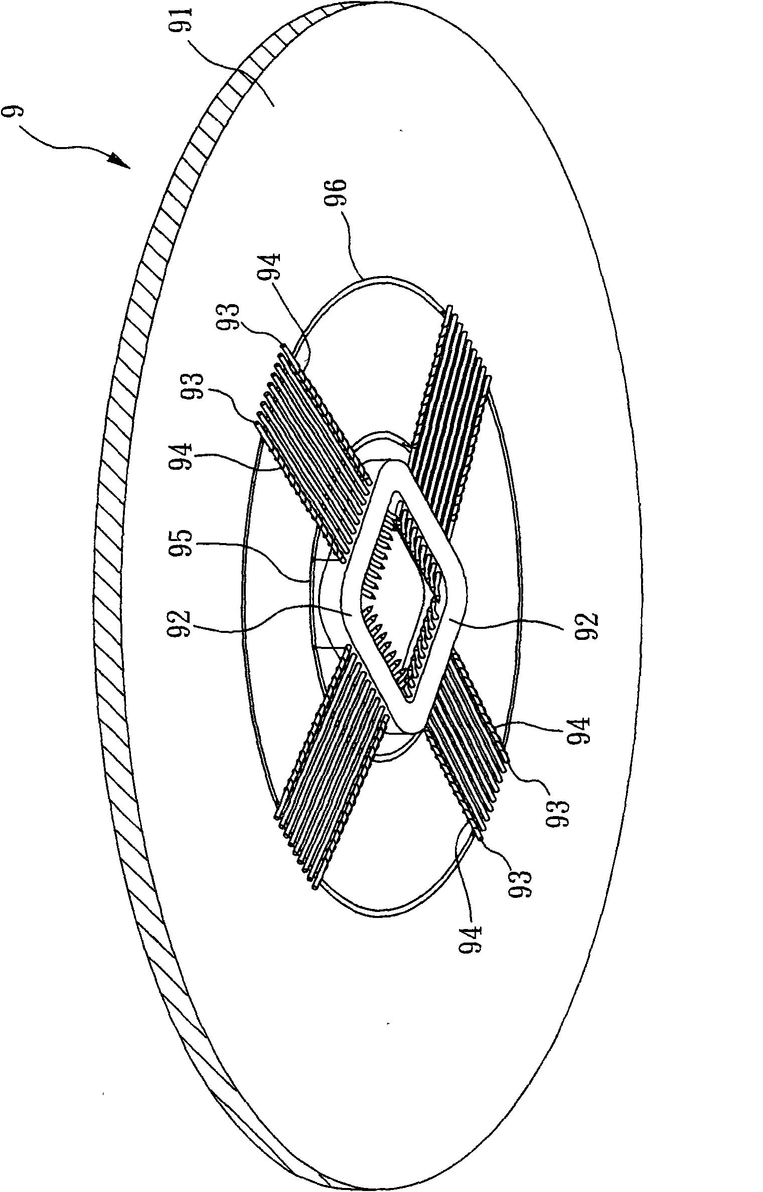
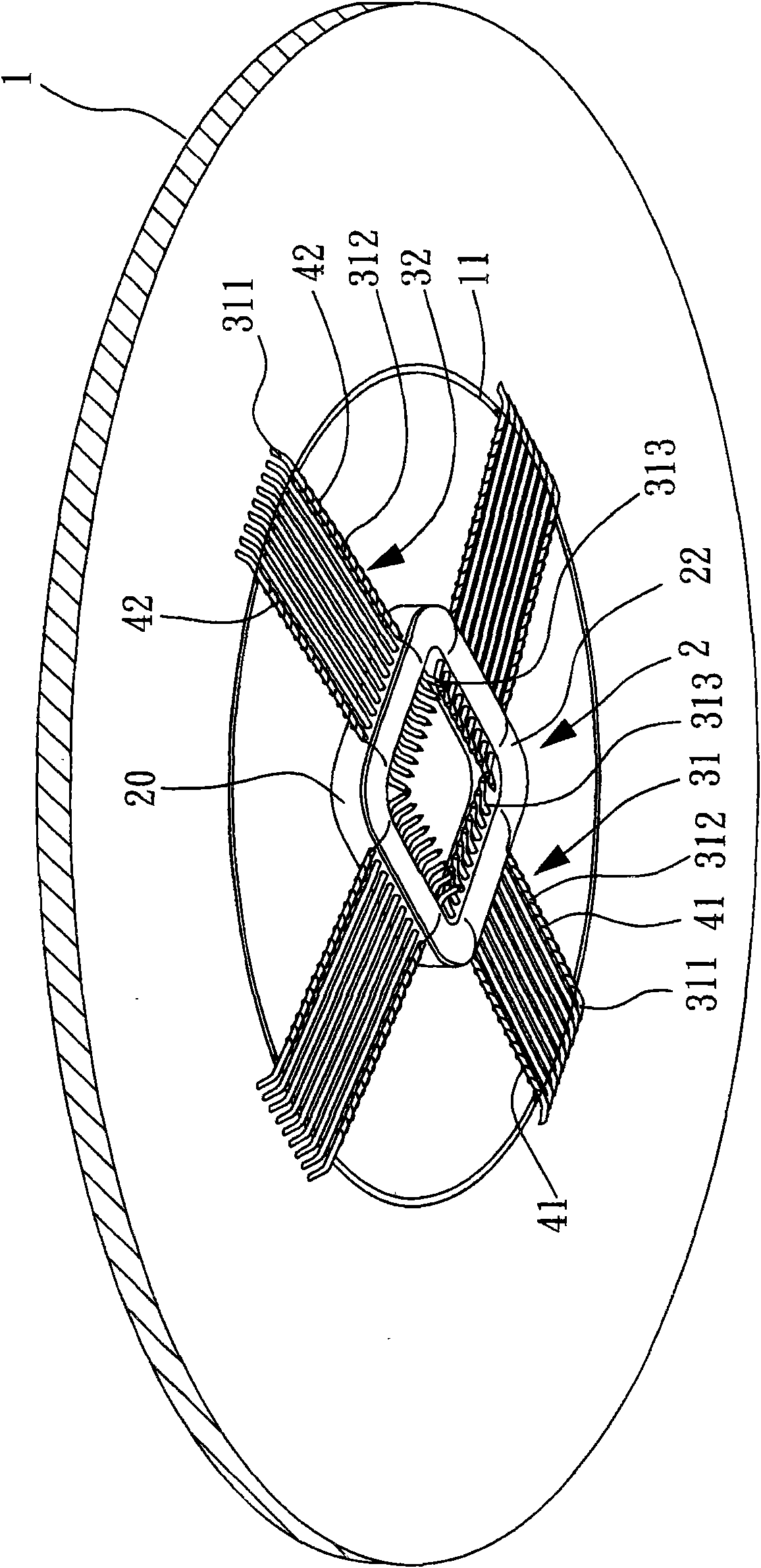
[0019] see also image 3 ,and Figure 4 . image 3 is a perspective view of a preferred embodiment of the probe card of the present invention, Figure 4 It is a cross-sectional view of a preferred embodiment of the probe card of the present invention.

[0020] As shown in the figure, the present invention relates to a probe card including a circuit board 1 , a probe holder 2 , at least one probe 31 , 32 , and at least one lead 41 , 42 .

[0021] The circuit board 1 includes a test circuit 10 and a ground circuit 11 . The probe seat 2 includes an insulating seat body 20, a conductive layer 22, and at least one conductive pin 23. One side of the insulating seat body 20 is fixedly arranged at the central part of the circuit board 1, and the other side is formed with a conductive layer 22, wherein , the insulating seat body 20 of the probe seat 2 refers to a hollow seat body, the conductive layer 22 refers to a hollow ring thin layer, in addition, the insulating seat body 20 o...


PUM


Abstract

The invention relates to a probe card. A conductive layer is arranged on an insulating base body of a probe seat of the probe card; and the conductive layer is electrically connected to a grounding circuit on the probe card through a conductive pin penetrating through the insulating base body, wherein the first end of a probe on the probe card is electrically connected to a test circuit of a circuit board; part of an intermediate section is fixed in the insulating base body in a penetrating way; the second end of the probe passes out of the insulating base body to expose outside; the periphery of the intermediate section of the probe is wound by a lead wire; the first end of the lead wire is electrically connected with the grounding circuit of the circuit board; and the second end is electrically connected with the conductive layer. Therefore, a section of grounding range of the conductive layer is added because of the wound lead wire of the probe, so that the inductance of a probe loop in the insulating base body can be reduced and the accuracy of test data of the probe is improved.

Description

technical field [0001] The present invention relates to a probe card, especially a probe card suitable for having a conductive layer. Background technique [0002] In the semiconductor wafer fabrication process, in order to test the quality of the die on the wafer, a test machine and a probe card must be used to perform the wafer test. The probe card has a precise contact mechanism to contact each die on the wafer, turn on the circuit, and perform electrical tests to ensure that the electrical characteristics and performance of the die are manufactured according to the design specifications. [0003] In recent years, the development of high-speed operation of semiconductor devices has become popular, so the test machine and the probe card must also be compatible with high frequency, but the traditional cantilever probe card is used in high-frequency testing, because the probes are adjacent to each other. Recently, the noise problem caused by electromagnetic interference oft...

Claims


Application Information

Patent Timeline
Patent Type & Authority Applications(China)
IPC IPC(8): G01R1/067G01R1/073
Inventor 倪建青陈冠州
Owner KING YUAN ELECTRONICS
Why Eureka
Try Eureka